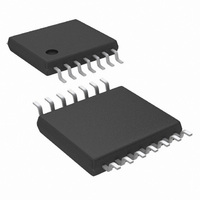
LM3150MH/NOPB National Semiconductor, LM3150MH/NOPB Datasheet - Page 8

LM3150MH/NOPB
Manufacturer Part Number
LM3150MH/NOPB
Description
IC REG SWITCH CTRL 6-42V 14TSSOP
Manufacturer
National Semiconductor
Series
PowerWise®, SIMPLE SWITCHER®r
Type
Step-Down (Buck)r
Datasheet
1.LM3150MHENOPB.pdf
(20 pages)
Specifications of LM3150MH/NOPB
Internal Switch(s)
No
Synchronous Rectifier
Yes
Number Of Outputs
1
Voltage - Output
Adj to 0.6V
Current - Output
12A
Frequency - Switching
1MHz
Voltage - Input
6 ~ 42 V
Operating Temperature
-40°C ~ 125°C
Mounting Type
Surface Mount
Package / Case
14-TSSOP Exposed Pad, 14-eTSSOP 14-HTSSOP
Package
14TSSOP EP
Output Voltage
0.6(Min) V
Output Current
12(Max) A
For Use With
551600142-002 - WEBENCH BUILD IT BOARD LM3150
Lead Free Status / RoHS Status
Lead free / RoHS Compliant
Power - Output
-
Other names
LM3150MH
Available stocks
Company
Part Number
Manufacturer
Quantity
Price
Company:
Part Number:
LM3150MH/NOPB
Manufacturer:
TI
Quantity:
11 235
Part Number:
LM3150MH/NOPB
Manufacturer:
TI/德州仪器
Quantity:
20 000
www.national.com
Theory of Operation
The LM3150 synchronous step-down SIMPLE SWITCHER
Controller utilizes a Constant On-Time (COT) architecture
which is a derivative of the hysteretic control scheme. COT
relies on a fixed switch on-time to regulate the output. The on-
time of the high-side switch can be set manually by adjusting
the size of an external resistor (R
constant switching frequency as V
tomatically adjusts the on-time inversely with the input volt-
age. Assuming an ideal system and V
1V, the following approximations can be made:
The on-time, t
Where constant K = 100 pC
The R
Where f
Control is based on a comparator and the on-timer, with the
output voltage feedback (FB) compared with an internal ref-
erence of 0.6V. If the FB level is below the reference, the high-
side switch is turned on for a fixed time, t
determined by the input voltage and the resistor R
ing this on-time, the switch remains off for a minimum off-time,
t
the FB pin voltage is below the reference, then the switch
turns on again for another on-time period. The switching will
continue in this fashion to maintain regulation. During contin-
uous conduction mode (CCM), the switching frequency ide-
ally depends on duty-cycle and on-time only. In a practical
application however, there is a small delay in the time that the
HG goes low and the SW node goes low that also affects the
switching frequency that is accounted for in the typical appli-
cation curves. The duty-cycle and frequency can be approx-
imated as:
Typical COT hysteretic controllers need a significant amount
of output capacitor ESR to maintain a minimum amount of
ripple at the FB pin in order to switch properly and maintain
efficient regulation. The LM3150 however, utilizes a propri-
etary Emulated Ripple Mode control scheme (ERM) that al-
lows the use of low ESR output capacitors. Not only does this
reduce the need for high output capacitor ESR, but also sig-
nificantly reduces the amount of output voltage ripple seen in
a typical hysteretic control scheme. The output ripple voltage
can become so low that it is comparable to voltage-mode and
current-mode control schemes.
OFF
, as specified in the Electrical Characteristics table or until
ON
s
resistance value can be calculated as follows:
is the desired switching frequency.
ON
:
ON
IN
). To maintain a relatively
varies, the LM3150 au-
IN
is much greater than
ON
ON
, which is
. Follow-
(1)
(2)
(3)
(4)
®
8
Programming the Output Voltage
The output voltage is set by two external resistors
(R
lows:
Where R
FB, and R
and GND.
Regulation Comparator
The feedback voltage at FB is compared to the internal ref-
erence voltage of 0.6V. In normal operation (the output volt-
age is regulated), an on-time period is initiated when the
voltage at FB falls below 0.6V. The high-side switch stays on
for the on-time, causing the FB voltage to rise above 0.6V.
After the on-time period, the high-side switch stays off until
the FB voltage falls below 0.6V.
Over-Voltage Comparator
The over-voltage comparator is provided to protect the output
from over-voltage conditions due to sudden input line voltage
changes or output loading changes. The over-voltage com-
parator continuously monitors the voltage at the FB pin and
compares it to a 0.72V internal reference. If the voltage at FB
rises above 0.72V, the on-time pulse is immediately termi-
nated. This condition can occur if the input or the output load
changes suddenly. Once the over-voltage protection is acti-
vated, the HG and LG signals remain off until the voltage at
FB pin falls below 0.72V.
Current Limit
Current limit detection occurs during the off-time by monitor-
ing the current through the low-side switch using an external
resistor, R
switch exceeds the user defined current limit value, the next
on-time cycle is immediately terminated. Current sensing is
achieved by comparing the voltage across the low side FET
with the voltage across the current limit set resistor R
voltage across R
are equal then the current limit comparator will terminate the
next on-time cycle.
The R
Where I
value, R
the expected maximum FET junction temperature, and I
TH
Figure 1 illustrates the inductor current waveform. During nor-
mal operation, the output current ripple is dictated by the
switching of the FETs. The current through the low-side
switch, I
and compared to the current limit, I
rent can be calculated as follows:
FB1
is an internal current supply of 85 µA typical.
,R
LIM
FB2
OCL
DS(ON)max
valley
FB2
value can be approximated as follows:
LIM
). The regulated output voltage is calculated as fol-
FB1
is the top resistor connected between VOUT and
is the user-defined average output current limit
, is sampled at the end of each switching cycle
. If during the off-time the current in the low-side
is the bottom resistor connected between FB
LIM
is the resistance value of the low-side FETat
and the voltage across the low-side FET
CL
, current. The valley cur-
LIM
. If the
LIM-
(5)
(6)
(7)


