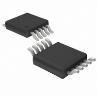
LT3750EMS#PBF Linear Technology, LT3750EMS#PBF Datasheet - Page 10

LT3750EMS#PBF
Manufacturer Part Number
LT3750EMS#PBF
Description
IC CTLR CAPACITOR CHARGE 10-MSOP
Manufacturer
Linear Technology
Type
Flyback, Forward Converterr
Datasheet
1.LT3750EMSPBF.pdf
(16 pages)
Specifications of LT3750EMS#PBF
Applications
Power Supply Controller
Mounting Type
Surface Mount
Package / Case
10-MSOP, Micro10™, 10-uMAX, 10-uSOP
Ic Function
Capacitor Charger Controller
Supply Voltage Range
3V To 24V
Operating Temperature Range
-40°C To +85°C
Digital Ic Case Style
MSOP
No. Of Pins
10
Msl
MSL 1 - Unlimited
Rohs Compliant
Yes
Lead Free Status / RoHS Status
Lead free / RoHS Compliant
Available stocks
Company
Part Number
Manufacturer
Quantity
Price
APPLICATIO S I FOR ATIO
Table 4. Recommended NMOS Transisitors
MANUFACTURER
Philips Semiconductor
(www.semiconductors.philips.com)
International Rectifier
(www.irf.com)
LT3750
The transistor’s continuous drain current rating must
exceed I
Table 4 lists recommended NMOS transistors.
Setting Current Limit
A sense resistor from the SOURCE pin to GND implements
current limit. The current limit is nominally 78mV/R
The average power dissipation rating of the current sense
resistor must exceed:
Additionally, there is approximately a 100ns propagation
delay from the time that peak current limit is detected to
when the gate transitions to the low state. This delay
increases the peak current limit by (V
Setting The Target Output Voltage
The parameters that determine the target output voltage
are the resistors R
transformer (N), and the voltage drop across the output
diode (V
to the following equation:
10
P
V
RESISTOR
OUT
AVG,M
DIODE
=
⎛
⎝ ⎜
1 24
). The target output voltage is set according
≥
.
.
I
PK
V
U
2
VOUT
•
•
R
R
3
R
VOUT
SENSE
BG
and R
U
•
N
⎛
⎜
⎝
BG
PSMN038-100K
⎞
⎠ ⎟
PART NUMBER
V
PHM21NQ15T
PHK12NQ10T
PHT6NQ10Y
OUT PK
, the turns ratio of the
–
W
IRF7488
IRF7493
IRF6644
V
TRANS
(
DIODE
V
OUT PK
)
+
)(t
N V
(
DELAY
•
U
)
T
R R ANS
)/L
I
SENSE
D
22.2
11.6
10.3
6.5
6.3
6.3
9.3
(A)
PRI
⎞
⎟
⎠
.
.
Use at least 1% tolerance resistors for R
Choosing large value resistors for R
amount of current that charges the parasitic internal
capacitances and degrades the response time of the V
comparator. This may result in overcharging of the output
capacitor. The maximum recommended value for R
2.5k for typical applications.
When high primary currents are used, a voltage spike
can prematurely trip the output voltage comparator. A
33pF to 100pF capacitor in parallel with R
filter this spike for most applications. Always check that
the voltage waveform on RBG does not overshoot and that
it reaches a plateau at maximum V
Discontinuous Mode Detection
The R
drain node. A 43k, 5% resistor is recommended for 300V
applications. Higher output voltages will require a larger
resistor.
In order for the LT3750 to properly detect discontinuous
mode and start a new charge cycle, the reflected voltage to
the primary winding must exceed the discontinuous mode
comparator threshold which is nominally 36mV. The
worst-case condition occurs when V
ground. When this occurs, the reflected voltage is simply
the diode forward voltage drop divided by N.
V
DS(MAX)
150
100
100
100
100
80
80
DCM
(V)
resistor stands off voltage transients on the
V
GS(MAX)
20
20
20
20
20
20
20
(V)
R
DS(ON)
10.7
55
28
90
38
29
15
OUT
(mΩ)
.
OUT
BG
BG
VOUT
decreases the
is sufficient to
is shorted to
PACKAGE
DirectFET
HVSON8
SOT223
SO-8
SO-8
SO-8
SO-8
and R
BG
3750fa
OUT
BG
is
.


