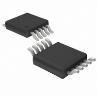
LT3750EMS#PBF Linear Technology, LT3750EMS#PBF Datasheet - Page 6

LT3750EMS#PBF
Manufacturer Part Number
LT3750EMS#PBF
Description
IC CTLR CAPACITOR CHARGE 10-MSOP
Manufacturer
Linear Technology
Type
Flyback, Forward Converterr
Datasheet
1.LT3750EMSPBF.pdf
(16 pages)
Specifications of LT3750EMS#PBF
Applications
Power Supply Controller
Mounting Type
Surface Mount
Package / Case
10-MSOP, Micro10™, 10-uMAX, 10-uSOP
Ic Function
Capacitor Charger Controller
Supply Voltage Range
3V To 24V
Operating Temperature Range
-40°C To +85°C
Digital Ic Case Style
MSOP
No. Of Pins
10
Msl
MSL 1 - Unlimited
Rohs Compliant
Yes
Lead Free Status / RoHS Status
Lead free / RoHS Compliant
Available stocks
Company
Part Number
Manufacturer
Quantity
Price
OPERATIO
LT3750
The LT3750 is designed to charge capacitors quickly and
efficiently. Operation can be best understood by referring
to Figures 1 and 2. Operation proceeds in four phases:
1. Start-up, 2. Primary-side charging, 3. Secondary en-
ergy transfer, 4. Discontinuous mode sensing.
1. Start-Up
Start-up occurs for approximately 20µs after the charge
pin is raised high. During this phase, a one-shot enables
the master latch and turns on the NMOS. The master latch
will remain in the set state until the target output voltage
is reached or a fault condition resets it.
6
(1c) Equivalent Circuit During Discontinuous Mode Detection
(1b) Equivalent Circuit During Secondary Energy
Transfer and Output Detection
(1a) Equivalent Circuit During Primary-Side Charging
V
V
V
TRANS
TRANS
TRANS
Figure 1. Equivalent Circuits
V
I
V
I
V
LPRI
I
LPRI
DRAIN
U
LPRI
DRAIN
DRAIN
+
–
+
–
+
–
•
•
•
+
–
+
–
+
–
V
S1
S1
V
V
S1
PRI
1:N
PRI
PRI
1:N
1:N
•
I
V
I
•
•
LSEC
V
I
V
LSEC
LSEC
SEC
SEC
+
–
SEC
+
–
+
–
S2
S2
S2
3750 F01c
3750 F01a
3750 F01b
2. Primary Side Charging
When the NMOS on latch is set, the gate driver rapidly
charges the gate pin to V
on forcing V
Consequently, current in the primary coil rises linearly at
V
DRAIN
I
I
V
LSEC
I
V
LPRI
I
PK
PK
N
SEC
PRI
V
–N (V
V
TRANS
PRIMARY-SIDE
TRANS
CHARGING
V
TRANS
DS(ON)
L
Figure 2. Idealized Charging Waveforms
– V
PRI
1.
– V
TRANS
DS(ON)
DS(ON)
– V
DS(ON)
– V
)
ENERGY TRANSFER
DS(ON)
AND OUTPUT
–(V
CC
SECONDARY
V
DETECTION
V
V
TRANS
OUT
OUT
OUT +
– 2V. The external NMOS turns
2.
L
across the primary winding.
+ V
+ V
N
SEC
+
V
V
DIODE
DIODE
DIODE
OUT
+ V
)
N
DISCONTINUOUS
DIODE
DETECTION
MODE
3.
V
TRANS
V
DS(ON)
3750 F02
3750fa


