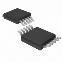
LT3750EMS#PBF Linear Technology, LT3750EMS#PBF Datasheet - Page 8

LT3750EMS#PBF
Manufacturer Part Number
LT3750EMS#PBF
Description
IC CTLR CAPACITOR CHARGE 10-MSOP
Manufacturer
Linear Technology
Type
Flyback, Forward Converterr
Datasheet
1.LT3750EMSPBF.pdf
(16 pages)
Specifications of LT3750EMS#PBF
Applications
Power Supply Controller
Mounting Type
Surface Mount
Package / Case
10-MSOP, Micro10™, 10-uMAX, 10-uSOP
Ic Function
Capacitor Charger Controller
Supply Voltage Range
3V To 24V
Operating Temperature Range
-40°C To +85°C
Digital Ic Case Style
MSOP
No. Of Pins
10
Msl
MSL 1 - Unlimited
Rohs Compliant
Yes
Lead Free Status / RoHS Status
Lead free / RoHS Compliant
Available stocks
Company
Part Number
Manufacturer
Quantity
Price
APPLICATIO S I FOR ATIO
Table 1. Recommended Transformers
MANUFACTURER
TDK
(www.tdk.com)
Sumida
(www.sumida.com)
Midcom
(www.midcom.com)
Coilcraft
(www.coilcraft.com)
LT3750
Safety Warning
Large capacitors charged to high voltage can deliver a
lethal amount of energy if handled improperly. It is par-
ticularly important to observe appropriate safety mea-
sures when designing the LT3750 into applications. First,
create a discharge circuit that allows the designer to safely
discharge the output capacitor. Second, adequately space
high voltage nodes from adjacent traces to satisfy printed
circuit board voltage breakdown requirements. High volt-
age nodes are the drain of the NMOS, the secondary side
of the transformer, and the output.
Transformer Selection
The flyback transformer is critical to proper operation of
the LT3750. It must be designed carefully so that it does
not cause excessive current or voltage on any pin of the
part.
As with all circuits, the LT3750 has finite bandwidth. In
order to give the LT3750 sufficient time to detect the
output voltage, observe the following restrictions on the
primary inductance:
otherwise, the LT3750 may overcharge the output.
Linear Technology has worked with several leading mag-
netic component manufacturers to produce flyback trans-
formers for use with the LT3750. Table 1 summarizes the
particular transformer characteristics.
8
L
PRI
≥
V
OUT
N I
•
•
PK
1
µs
U
DCT15EFD-U44S003
DCT20EFD-U32S003
PART NUMBER
C8118 Rev P1
C8117 Rev P1
C8119 Rev P1
DA2032-AL
DA2033-AL
DA2034-AL
U
32050
32051
32052
W
SIZE L × W × H (mm)
17.4 × 24.1 × 10.2
22.5 × 16.5 × 8.5
23 × 18.6 × 10.8
28.7 × 22 × 11.4
28.7 × 22 × 11.4
20.6 × 30 × 11.3
23.1 × 18 × 9.4
17.2 × 22 × 8.9
32.3 × 27 × 14
30 × 22 × 12
21 × 14 × 8
U
MAXIMUM I
Switching Period
The LT3750 employs an open-loop control scheme caus-
ing the switching period to decrease with output voltage.
Typical switching frequency is between 100kHz to 300kHz.
Figure 3 shows typical switching period in an application
with a 3A peak current.
Output Diode Selection
When choosing the rectifying diode, ensure its peak
repetitive forward current rating exceeds the peak cur-
rent (I
rating exceeds V
through the diode varies during the charge cycle because
the switching period decreases as V
average current through the diode is greatest when the
10
10
10
10
5
3
5
3
5
3
5
PK
PRI
/N) and that the peak repetitive reverse voltage
Figure 3. Typical Switching Period vs V
20
16
12
(A)
8
4
0
0
OUT
50
+ (N)(V
100
L
PRI
V
10
10
10
10
10
10
10
10
10
10
10
OUT
(µH)
150
TRANS
(V)
200
). The average current
250
TURNS RATIO (PRI:SEC)
OUT
3750 F03
increases. The
300
OUT
1:10
1:10
1:10
1:10
1:10
1:10
1:10
1:10
1:10
1:10
1:10
3750fa


