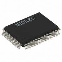
KSZ8995XA Micrel Inc, KSZ8995XA Datasheet - Page 14

KSZ8995XA
Manufacturer Part Number
KSZ8995XA
Description
IC SWITCH 10/100 5PORT 128PQFP
Manufacturer
Micrel Inc
Specifications of KSZ8995XA
Applications
*
Mounting Type
Surface Mount
Package / Case
128-MQFP, 128-PQFP
Number Of Primary Switch Ports
5
Internal Memory Buffer Size
64
Operating Supply Voltage (typ)
1.8/2.5/3.3V
Fiber Support
Yes
Integrated Led Drivers
Yes
Phy/transceiver Interface
MII/SNI
Power Supply Type
Analog/Digital
Package Type
PQFP
Data Rate (typ)
10/100Mbps
Vlan Support
Yes
Operating Temperature (max)
70C
Operating Temperature (min)
0C
Pin Count
128
Mounting
Surface Mount
Jtag Support
No
Operating Temperature Classification
Commercial
Lead Free Status / RoHS Status
Lead free / RoHS Compliant
For Use With
576-1642 - BOARD EVALUATION FOR KSZ8995XA
Lead Free Status / RoHS Status
Compliant, Lead free / RoHS Compliant
Other names
576-1042
Available stocks
Company
Part Number
Manufacturer
Quantity
Price
Company:
Part Number:
KSZ8995XA
Manufacturer:
MICREL
Quantity:
1 334
Company:
Part Number:
KSZ8995XA
Manufacturer:
MICREL30
Quantity:
348
Part Number:
KSZ8995XA
Manufacturer:
MICREL
Quantity:
20 000
KS8995XA
Notes:
1. P = Power supply.
2. PU = Strap pin pull-up.
M9999-051305
Pin Number
I = Input.
O = Output.
I/O = Bidirectional.
Gnd = Ground.
Ipu = Input w/internal pull-up.
Ipd = Input w/internal pull-down.
Ipd/O = Input w/internal pull-down during reset, output pin otherwise.
Ipu/O = Input w/internal pull-up during reset, output pin otherwise.
PD = Strap pull-down.
107
108
114
113
96
95
94
93
92
91
90
45
46
68
67
60
65
64
63
62
61
66
57
55
54
53
52
51
56
NC / MUX1
NC / MUX2
Pin Name
PMRXDV
PMRXER
PMRXD0
PMRXD1
PMRXD2
PMRXD3
PMTXEN
PMTXER
PMTXD0
PMTXD1
PMTXD2
PMTXD3
PMRXC
PMTXC
LED3-2
LED4-0
LED4-1
LED4-2
LED5-0
LED5-1
LED5-2
PCOL
PCRS
MDIO
MDC
PS0
PS1
Type
Ipu/O
Ipu/O
Ipu/O
Ipu/O
Ipu/O
Ipu/O
Ipu/O
Ipu/O
Ipd/O
Ipd/O
Ipd/O
Ipd/O
Ipd/O
Ipd/O
Ipd/O
Ipd/O
Ipu
Ipd
Ipd
Ipd
Ipd
Ipd
Ipd
Ipd
Ipd
O
O
(1)
Port
All
All
3
4
4
4
5
5
5
5
5
5
5
5
5
5
5
5
5
5
5
5
5
5
5
I
I
Pin Function
LED indicator 2.
LED indicator 0.
LED indicator 1.
LED indicator 2.
LED indicator 0.
LED indicator 1. Strap option: PU (default): enable PHY MII I/F
Pd: tristate all PHY MII output. See “Pin# 86 SCONF1.”
LED indicator 2. Aging setup. See “Aging” section.
Switch or PHY[5] MII management data clock.
Switch or PHY[5] MII management data I/O.
No connect. Factory test pin.
No connect. Factory test pin.
PHY[5] MII collision detect/ Force flow control. See “Register 18.”
PHY[5] MII carrier sense/Force duplex mode. See “Register 28.”
PHY[5] MII receive clock. PHY mode MII.
PHY[5] MII receive bit 0. Strap option: PD (default) = disable
aggressive back-off algorithm in half-duplex mode; PU = enable for
performance enhancement.
PHY[5] MII receive bit 1. Strap option: PD (default) = drop excessive
collision packets; PU = does not drop excessive collision packets.
PHY[5] MII receive bit 2. Strap option: PD (default) = disable back
pressure; PU = enable back pressure.
PHY[5] MII receive bit 3. Strap option: PD (default) = enable flow
control; PU = disable flow control.
PHY[5] MII receive data valid.
PHY[5] MII receive error. Strap option: PD (default) = packet size 1518/
1522 bytes; PU = 1536 bytes.
PHY[5] MII transmit clock. PHY mode MII.
PHY[5] MII transmit bit 0.
PHY[5] MII transmit bit 1.
PHY[5] MII transmit bit 2.
PHY[5] MII transmit bit 3.
PHY[5] MII transmit enable.
PHY[5] MII transmit error.
No connect or pull down.
No connect or pull down.
14
(2)
Micrel, Inc.
May 2005


