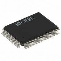
KSZ8995XA Micrel Inc, KSZ8995XA Datasheet - Page 23

KSZ8995XA
Manufacturer Part Number
KSZ8995XA
Description
IC SWITCH 10/100 5PORT 128PQFP
Manufacturer
Micrel Inc
Specifications of KSZ8995XA
Applications
*
Mounting Type
Surface Mount
Package / Case
128-MQFP, 128-PQFP
Number Of Primary Switch Ports
5
Internal Memory Buffer Size
64
Operating Supply Voltage (typ)
1.8/2.5/3.3V
Fiber Support
Yes
Integrated Led Drivers
Yes
Phy/transceiver Interface
MII/SNI
Power Supply Type
Analog/Digital
Package Type
PQFP
Data Rate (typ)
10/100Mbps
Vlan Support
Yes
Operating Temperature (max)
70C
Operating Temperature (min)
0C
Pin Count
128
Mounting
Surface Mount
Jtag Support
No
Operating Temperature Classification
Commercial
Lead Free Status / RoHS Status
Lead free / RoHS Compliant
For Use With
576-1642 - BOARD EVALUATION FOR KSZ8995XA
Lead Free Status / RoHS Status
Compliant, Lead free / RoHS Compliant
Other names
576-1042
Available stocks
Company
Part Number
Manufacturer
Quantity
Price
Company:
Part Number:
KSZ8995XA
Manufacturer:
MICREL
Quantity:
1 334
Company:
Part Number:
KSZ8995XA
Manufacturer:
MICREL30
Quantity:
348
Part Number:
KSZ8995XA
Manufacturer:
MICREL
Quantity:
20 000
Broadcast Storm Protection
The KS8995XA has an intelligent option to protect the switch system from receiving too many broadcast packets. Broadcast
packets will be forwarded to all ports except the source port, and thus use too many switch resources (bandwidth and available
space in transmit queues). The KS8995XA has the option to include “multicast packets” for storm control. The broadcast storm
rate parameters are programmed globally, and can be enabled or disabled on a per port basis. The rate is based on a 50ms
interval for 100BT and a 500ms interval for 10BT. At the beginning of each interval, the counter is cleared to zero, and the rate
limit mechanism starts to count the number of bytes during the interval. The rate definition is described in Register 6 and
Register 7. The default setting for registers 6 and 7 is 0x4A, which is 74 decimal. This is equal to a rate of 1%, calculated as
follows:
MII Interface Operation
The media independent interface (MII) is specified by the IEEE 802.3 committee and provides a common interface between
physical layer and MAC layer devices. The KS8995XA provides two such interfaces. The MII-P5 interface is used to connect
to the fifth PHY, whereas the MII-SW interface is used to connect to the fifth MAC. Each of these MII interfaces contains two
distinct groups of signals, one for transmission and the other for receiving. The table below describes the signals used in the
MII-P5 interface.
The MII-P5 interface operates in PHY mode only, while the MII-SW interface operates in either MAC mode or PHY mode. These
interfaces are nibble-wide data interfaces and therefore run at 1/4 the network bit rate (not encoded). Additional signals on the
transmit side indicate when data is valid or when an error occurs during transmission. Likewise, the receive side has indicators
that convey when the data is valid and without physical layer errors. For half-duplex operation, there is a signal that indicates
a collision has occurred during transmission.
Note that the signal MRXER is not provided on the MII-SW interface for PHY mode operation and the signal MTXER is not
provided on the MII-SW interface for MAC mode operation. Normally MRXER would indicate a receive error coming from the
physical layer device. MTXER would indicate a transmit error from the MAC device. These signals are not appropriate for this
configuration. For PHY mode operation, if the device interfacing with the KS8995XA has an MRXER pin, it should be tied low.
For MAC mode operation, if the device interfacing with the KS8995XA has an MTXER pin, it should be tied low.
May 2005
KS8995XA
148,800 frames/sec × 50ms/interval × 1% = 74 frames/interval (approx.) = 0x4A
MII Signal
MRXDV
MRXER
MTXEN
MTXER
MRXD3
MRXD2
MRXD1
MRXD0
MTXD3
MTXD2
MTXD1
MTXD0
MCRS
MRXC
MTXC
MCOL
MDIO
MDC
Table 1. MII – P5 Signals (PHY Mode)
Management data clock
Management data I/O
Transmit data bit 3
Transmit data bit 2
Transmit data bit 1
Transmit data bit 0
Collision detection
Receive data valid
Receive data bit 3
Receive data bit 2
Receive data bit 1
Receive data bit 0
Transmit enable
Transmit clock
Transmit error
Receive clock
Carrier sense
Receive error
Description
23
KS8995XA Signal
PMRXD[3]
PMRXD[2]
PMRXD[1]
PMRXD[0]
PMTXD[3]
PMTXD[2]
PMTXD[1]
PMTXD[0]
PMRXDV
PMRXER
PMTXEN
PMTXER
PMRXC
PMTXC
PCOL
PCRS
MDIO
MDC
M9999-051305
Micrel, Inc.


