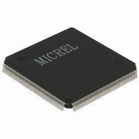
KS8695X Micrel Inc, KS8695X Datasheet - Page 23

KS8695X
Manufacturer Part Number
KS8695X
Description
IC SWITCH 10/100 5PORT 208PQFP
Manufacturer
Micrel Inc
Datasheet
1.KS8695X.pdf
(39 pages)
Specifications of KS8695X
Applications
*
Mounting Type
Surface Mount
Package / Case
208-MQFP, 208-PQFP
For Use With
KS8695-EVAL - EVAL KIT EXPERIMENTAL KS8695576-1005 - BOARD EVAL EXPERIMENT KS8695X
Lead Free Status / RoHS Status
Lead free / RoHS Compliant
Available stocks
Company
Part Number
Manufacturer
Quantity
Price
Factory Test Pins
Note:
1. I = Input.
October 2004
KS8695X
O/I = Output in normal mode; input pin during reset.
O = Output.
119
118
117
197
149
Pin
Pin
78
81
82
85
89
88
87
86
TICTESTENN
TESTREQB
TESTREQA
WRSTPLS
TESTACK
ERWEN0/
ERWEN1/
ERWEN2/
ERWEN3/
B0SIZE0
B0SIZE1
TESTEN
EWAITN
RCSN[1]
RCSN[0]
EROEN/
WLED0/
WLED1/
TEST1
TEST2
Name
Name
I/O Type
I/O Type
O/I
O/I
O/I
O
O
O
O
O
I
I
I
I
(1)
(1)
Description
External wait: Active low. This signal is asserted when an external I/O device or a
ROM/SRAM/FLASH bank needs more access cycles than those defined in the
corresponding control register.
ROM/SRAM/FLASH chip select: Active low. The KS8695X can access up to two
external ROM/SRAM/FLASH memory banks. The RCSN pins can be controlled to
map the CPU addresses into physical memory banks.
Normal mode: External I/O and ROM/SRAM/FLASH output enable: Active low.
When asserted, this signal controls the output enable port of the specified memory
device.
During reset: Watchdog timer reset polarity setting. WRSTPLS=0, Active low;
WRSTPLS = 1, active high. No default.
External I/O and ROM/SRAM/FLASH write byte enable: Active low. When asserted,
the ERWENx controls the byte write enable of the memory device (except SDRAM).
ARM CPU test signal (factory test signal).
External I/O and ROM/SRAM/FLASH write byte enable: Active low. When asserted,
the ERWENx controls the byte write enable of the memory device (except SDRAM).
ARM CPU test signal (factory test signal).
External I/O and ROM/SRAM/FLASH write byte enable: Active low. When asserted,
the ERWENx controls the byte write enable of the memory device except SDRAM).
ARM CPU test signal (factory test signal).
External I/O and ROM/SRAM/FLASH write byte enable. Active low. When asserted,
the ERWENx controls the byte write enable of the memory device (except SDRAM).
ARM CPU test signal (factory test signal).
Normal mode: WAN LED indicator 0: Programmable via WAN misc. Control register
bits [2:0].
000 = Speed; 001 = Link; 010 = Full/half duplex; 011 = Collision;
100 = TX/RX activity; 101 = Full-duplex collision; 110 = Link/Activity.
During reset: Bank 0 data access size. Bank 0 is used for the boot program.
B0SiZE[1:0] are used to specify the size of the bank 0 data bus width as follows:
‘01’ = one byte, ‘10’ = half-word, ‘11’ = one word, and ‘00’ = reserved.
Normal mode: WAN LED indicator 1: Programmable via WAN Misc. Control register
bits [6:4].
000 = Speed; 001 = Link; 010 = Full/half duplex; 011 = Collision;
100 = TX/RX activity; 101 = Full-duplex collision; 110 = Link/Activity.
During reset: Bank 0 data access size. Bank 0 is used for the boot program.
B0SIZE[1:0] are used to specify the size of the bank 0 data bus width as follows:
‘01’ = one byte, ‘10’ = half-word, ‘11’ = one word, and ‘00’ = reserved.
Description
Chip test enable: (factory test signal), pull down if not used.
PHY test pin: (factory test signal).
PHY test pin: (factory test signal).
23
M9999-102604
Micrel


