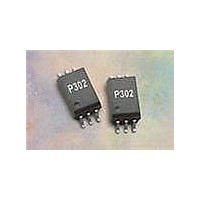
ACPL-P302-000E Avago Technologies US Inc., ACPL-P302-000E Datasheet - Page 13

ACPL-P302-000E
Manufacturer Part Number
ACPL-P302-000E
Description
OPTOCOUPLER W/GAASP LED 6-SOIC
Manufacturer
Avago Technologies US Inc.
Datasheet
1.ACPL-P302-500E.pdf
(14 pages)
Specifications of ACPL-P302-000E
Output Type
Push-Pull, Totem-Pole
Package / Case
SO-6
Voltage - Isolation
3750Vrms
Number Of Channels
1, Unidirectional
Current - Output / Channel
400mA
Propagation Delay High - Low @ If
300ns @ 7mA
Current - Dc Forward (if)
12mA
Input Type
DC
Mounting Type
Surface Mount
Fall Time
50 ns
Rise Time
50 ns
Configuration
1 Channel
Isolation Voltage
3750 Vrms
Maximum Forward Diode Voltage
1.8 V
Minimum Forward Diode Voltage
1.2 V
Maximum Reverse Diode Voltage
5 V
Maximum Forward Diode Current
12 mA
Maximum Power Dissipation
250 mW
Maximum Operating Temperature
+ 100 C
Minimum Operating Temperature
- 40 C
Number Of Elements
1
Forward Voltage
1.8V
Forward Current
25mA
Operating Temp Range
-40C to 100C
Power Dissipation
250mW
Propagation Delay Time
700ns
Pin Count
6
Mounting
Surface Mount
Reverse Breakdown Voltage
5V
Operating Temperature Classification
Industrial
Lead Free Status / RoHS Status
Lead free / RoHS Compliant
Lead Free Status / RoHS Status
Lead free / RoHS Compliant, Lead free / RoHS Compliant
Dead Time and Propagation Delay Specifications
The ACPL-P302/W302 includes a Propagation Delay Dif-
ference (PDD) specification intended to help designers
minimize “dead time” in their power inverter designs.
Dead time is the time high and low side power transistors
are off. Any overlap in Ql and Q2 conduction will result in
large currents flowing through the power devices from
the high voltage to the low-voltage motor rails. To mini-
mize dead time in a given design, the turn on of LED2
should be delayed (relative to the turn off of LED1) so that
under worst-case conditions, transistor Q1 has just turned
off when transistor Q2 turns on, as shown in Figure 24.
The amount of delay necessary to achieve this condition
is equal to the maximum value of the propagation delay
difference specification, PDD max, which is specified to be
500 ns over the operating temperature range of -40° to
100°C.
Figure 24. Minimum LED Skew for Zero Dead Time.
13
*PDD = PROPAGATION DELAY DIFFERENCE
NOTE: FOR PDD CALCULATIONS THE PROPAGATION DELAYS
ARE TAKEN AT THE SAME TEMPERATURE AND TEST CONDITIONS.
V
V
I
I
OUT1
OUT2
LED1
LED2
PDD* MAX = (t
t
PHL MAX
Q2 OFF
Q1 ON
t
PLH MIN
PHL
- t
PLH
)
MAX
= t
Q1 OFF
Q2 ON
PHL MAX
- t
PLH MIN
*PDD = PROPAGATION DELAY DIFFERENCE
NOTE: FOR DEAD TIME AND PDD CALCULATIONS ALL PROPAGATION
DELAYS ARE TAKEN AT THE SAME TEMPERATURE AND TEST CONDITIONS.
V
V
I
I
Delaying the LED signal by the maximum propagation
delay difference ensures that the minimum dead time is
zero, but it does not tell a designer what the maximum
dead time will be. The maximum dead time is equivalent
to the difference between the maximum and minimum
propagation delay difference specification as shown in
Figure 25. The maximum dead time for the ACPL-P302/
W302 is 1 μs (= 0.5 μs - (-0.5 μs)) over the operating tem-
perature range of –40°C to 100°C.
Note that the propagation delays used to calculate PDD
and dead time are taken at equal temperatures and test
conditions since the optocouplers under consideration
are typically mounted in close proximity to each other and
are switching identical IGBTs.
OUT1
OUT2
Figure 25. Waveforms for Dead Time.
LED1
LED2
(t
PHL-
PDD* MAX
Q1 ON
Q2 OFF
t
t
PHL MIN
PHL MAX
t
PLH
)
MAX
MAXIMUM DEAD TIME
(DUE TO OPTOCOUPLER)
= (t
= (t
= PDD* MAX – PDD* MIN
PHL MAX
PHL MAX
t
MIN
PLH
t
PLH MAX
- t
- t
PHL MIN
PLH MIN
) + (t
) – (t
Q1 OFF
PLH MAX
PHL MIN
Q2 ON
- t
- t
PLH MAX
PLH MIN
)
)


