20-101-0303 Rabbit Semiconductor, 20-101-0303 Datasheet
20-101-0303
Specifications of 20-101-0303
20-101-303
20-101-303
316-1175


Related parts for 20-101-0303


20-101-0303 Summary of contents
Page 1
... OP7100 Serial Graphic Display User’s Manual 019–0065 • 070831–O ...
Page 2
... Part Number 019-0065 • 070831-O • Printed in U.S.A. © 1999–2007 Rabbit Semiconductor Inc. • All rights reserved. Rabbit Semiconductor reserves the right to make changes and improvements to its products without providing notice. No part of the contents of this manual may be reproduced or transmitted in any form or by any means without the express written permission of Rabbit Semiconductor ...
Page 3
... Development and Evaluation Tools ..................................................... 14 Software .......................................................................................... 14 CE Compliance .................................................................................... 15 Chapter 2: Getting Started Initial OP7100 Setup ............................................................................ 18 Parts Required ................................................................................. 18 Setting Up the OP7100 ................................................................... 18 Connecting the OP7100 to a Host PC .................................................. 20 Running Dynamic C ............................................................................. 22 Chapter 3: Hardware OP7100 Subsystems Overview ............................................................ 24 Computing Module ......................................................................... 24 Power Management ............................................................................. 25 ADM691 Supervisor Chip .............................................................. 26 Handling Power Fluctuations ........................................................ 26 Watchdog Timer ...
Page 4
... FE (Framing Error) ....................................................................... 46 PE (Parity Error) ........................................................................... 46 OVRN (Overrun Error) ................................................................ 46 RDRF (Receiver Data Register Full) ............................................ 46 ASCI Control Register A ................................................................ 47 MOD0–MOD2 (Data Format Mode Bits) .................................... 47 MPBR/EFR (Multiprocessor Bit Receive/Error Flag Reset) ........ 47 /RTS0 (Request to Send, Channel 0) ............................................ 47 CKA1D (CKA1 Disable) .............................................................. 47 TE (Transmitter Enable) ............................................................... 47 RE (Receiver Enable) ................................................................... 48 MPE (Multiprocessor Enable) ...
Page 5
Dynamic C 32 Libraries ....................................................................... 56 OP71HW.LIB .................................................................................. 56 Keypad Programming ..................................................................... 65 Using Dynamic C v. 5.xx ..................................................................... 66 EZIOOP71.LIB ............................................................................... 66 GLCD.LIB ...................................................................................... 66 KP_OP71.LIB ................................................................................. 70 SYS.LIB .......................................................................................... 72 Upgrading Dynamic C ......................................................................... 73 New LCD Controller ...
Page 6
... OP7100 Memory ............................................................................... 100 Execution Timing .......................................................................... 101 Memory Map ..................................................................................... 102 Input/Output Select Map ............................................................... 102 Z180 Internal Input/Output Registers Addresses 00-3F ................ 102 Epson 72423 Timer Registers 0x4180–0x418F ............................ 104 Other Registers .............................................................................. 105 Interrupt Vectors ................................................................................ 106 Power-Failure Interrupts ............................................................... 107 Interrupt Priorities ......................................................................... 107 Appendix D: Serial Interface Board Introduction ...
Page 7
... Instructions are also provided for using Dynamic C functions. Assumptions Assumptions are made regarding the user's knowledge and experience in the following areas. • Ability to design and engineer the target system that interfaces with the OP7100. • Understanding the basics of operating a software program and editing files under Windows on a PC. ...
Page 8
Acronyms Table 1 lists and defines the acronyms that may be used in this manual. Acronym EPROM Erasable Programmable Read-Only Memory EEPROM Electronically Erasable Programmable Read-Only Memory LCD Liquid Crystal Display LED Light-Emitting Diode NMI Nonmaskable Interrupt PIO Parallel Input/Output ...
Page 9
... An ellipsis indicates that (1) irrelevant program text is omitted for brevity or that (2) preceding program text may be repeated indefinitely Brackets function’s definition or program segment indicate that the enclosed directive is optional. < > Angle brackets occasionally enclose classes of terms vertical bar indicates that a choice should be made from among the items listed ...
Page 10
About This Manual OP7100 ...
Page 11
Chapter 1 provides an overview and a brief description of the OP7100 features. OP7100 HAPTER VERVIEW Overview 11 ...
Page 12
... The OP7100 display terminal uses display technologies that require mini- mal mounting depth and offer maximum viewing angles. The memory allows application-screen bitmaps (240 × 320 stored with- out compression in a 256K flash EPROM. A further 256K is available for the application in a second flash EPROM. ...
Page 13
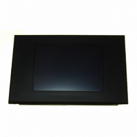
... Features The OP7100 includes the following features. • 240 × 320 ¼ VGA LCD (with touchscreen on OP7100 only) • jumper-selectable background—positive (blue images on white background) or negative (white images on blue background) • software-controlled cold-cathode fluorescent backlighting • software-controlled contrast is enabled/disabled with jumper settting • ...
Page 14
... For ordering information, call your Rabbit Semiconductor Sales Representative. Software The OP7100 is programmed using Rabbit Semiconductor’s Dynamic C, an integrated development environment that includes an editor compiler, and a debugger. Library functions provide an easy and robust interface to the OP7100. Rabbit Semiconductor’s Dynamic C reference manuals provide complete software descriptions and programming instructions ...
Page 15
... OP7100 into your application to comply with CE requirements. • The power supply provided with the Tool Kit is for development purpose only the customer’s responsibility to provide a CE compliant power supply for their end-product application. • The OP7100 has been tested to meet the following immunity standards. ...
Page 16
Overview OP7100 ...
Page 17
C Chapter 2 provides instructions for connecting the OP7100 to a host PC and running a sample program. OP7100 G 2: ETTING HAPTER S TARTED Getting Started 17 ...
Page 18
... Initial OP7100 Setup Parts Required • unregulated DC power supply capable of delivering up to 1.1 A • Serial cable The necessary parts are supplied with the Tool Kit. Setting Up the OP7100 1. Remove the green power connector shown in Figure 2-1 from the back of the OP7100. ...
Page 19
Figure 2-2. OP7100 Demo Screens OP7100 SUPPORT Getting Started 19 ...
Page 20
... SIB. An RJ-12 to DB9 adapter is included for DB9 PC COM ports. Remove any jumpers that may be installed on the OP7100’s header J4 and plug the SIB’s 8-pin connector onto header J4 as shown in Figure 2-4. Make sure that pin 1 on the ribbon cable connector (on the striped side) matches up with pin (indicated by a small white circle next to the header) ...
Page 21
... Figure 2-4. SIB Programming Connection Figure 2-5. Direct Programming Connection Option 2 uses an RS-232 serial port to program the OP7100. If this serial port is needed in your application, use the SIB as described in Option 1. See Chapter 3, “Hardware,” for more information on the serial ports. OP7100 Pin 1 Marked ...
Page 22
... Serial Options OP7100 both set their baud rate automatically to match the communication rate set on the host PC using Dynamic C (9600 bps, 19,200 bps, 28,800 bps, or 57,600 bps). To begin, adjust the communications rate to 19,200 bps. Make sure that the PC serial port used to connect the serial cable (COM1 or COM2) is the one selected in the Dynamic C the 1-stop-bit protocol ...
Page 23
... Chapter 3 describes how to use the OP7100. Sections are included to describe the following features. • Subsystems Overview • Power Management • Liquid Crystal Display • Keyboard Interface • Digital I/O • Serial Communication OP7100 HAPTER ARDWARE Hardware 23 ...
Page 24
... The simulated EEPROM in the OP7100 is unused at the present time, but addresses 0 and 1 are reserved for furture use. Do not use these addresses in your application. 24 Hardware SRAM Flash1 ’691 super. LCD Control VRAM1 EPLD Backlight Buzzer Optional Software Contrast Adjustment RTC Flash2 VRAM2 LCD 320 x 240 Contrast Adjustment OP7100 ...
Page 25
... DE-9 connector, by installing a 0 Ω resistor at R32. This option allows power to be supplied to a serial device connected to the OP7100 as long as the serial device’s RS-232 port can handle the DC input on pin 9. Be sure to use a power supply with sufficient capacity (for example, 1 handle surges when the OP7100 and any devices connected to it are first turned on ...
Page 26
... Also, depending on the number of fluctuations of the DC input (and hence, the number of stacked power- failure interrupts), the processor’s stack can overflow, possibly into your program’s code or data. The following sample program shows how to handle a power-failure interrupt ...
Page 27
... To increase reliability, the ADM691’s watchdog timer forces a system reset if a program does not notify the supervisor nominally at least every second. The assumption is that if the program fails to “hit” the watchdog, the program must be stuck in a loop or halted. The Dynamic C function for hitting the ...
Page 28
... Power Shutdown and Reset When VCC (+5 V) drops below V ADM691 supervisor asserts V and stays that way for at least 50 ms. This delay allows the system’s MIN devices to power up and stabilize before the CPU starts. PFI “Early Warning” When drops below 1.3 V ± 0.05 V (i.e., DCIN drops below ~10 V), ...
Page 29
... VRAM, the voltage supplied to the RAM and RTC, can also protect other devices attached to the system against power failures. The ADM691 super- visor switches VRAM to VBAT or VCC, whichever is greater. (To prevent “hunting,” the switchover actually occurs when Vcc higher than VBAT.) The circuit draws no current from the battery once regular power is applied. ...
Page 30
... Liquid Crystal Display (LCD) The 240 × 320 ¼ VGA LCD supports both graphics and text. Automatic contrast control is built in so that the contrast, once set, does not drift as the OP7100 warms moved. Figure 3-4 provides a block diagram of the LCD control and RAM circuits. ...
Page 31
Figure 3-6 shows the jumper settings for the contrast control options. Figure 3-6. Contrast Control Jumper Configurations Background The OP7100 comes factory-configured to display blue characters on a white (positive) background. The jumpers on header JP1 may be rear- ranged ...
Page 32
Coordinate Systems Figure 3-8 shows the coordinate systems for the touchscreen and the LCD. Figure 3-8. Coordinate Systems LCD Controller Chip The LCD controller chip provides support for the LCD module. The controller chip is attached to the data bus ...
Page 33
... Other functions support the LCD module to adjust its contrast and to turn the white CCFL backlight on and off. A variable resistor between two of the LCD module’s terminals sets the contrast, which is set either by soft- ware or manually, depending on the jumper setting on header JP2. Once a contrast value is set, it will be maintained ...
Page 34
Keypad Interface The OP7100 has a touchscreen, which is connected to the circuit board at header J5. Header J6 is available for a customer-supplied keypad for the OP7110. Table 3-1 lists the pinouts for headers J5 and J6. The pinout ...
Page 35
Digital I/O The OP7100 has eight CMOS/TTL-level digital inputs and eight CMOS/ TTL-level digital outputs. The digital inputs are provided with pullup resistors, shown in Figure 3-12, to provide a known state before a digital input is applied.. Figure 3-12. ...
Page 36
Serial Communication Two serial channels support asynchronous communication at baud rates from 300 bps to 57,600 bps. Serial communication provides a simple and robust means for networking controllers and other devices. Figure 3-14 illustrates the configuration of the OP7100 serial ...
Page 37
... The jumpers on header JP4 may be reconfigured so that header J11 carries the Z180 Port 1 TX1 and RX1 RS-232 signals on pins 2 and 3 instead of the factory-default RS-485+ and RS-485– signals. Figure 3-16 shows the header JP4 jumper configurations and the location of headers JP3 and JP4. ...
Page 38
... Monitoring and reading a circular receive buffer. • Monitoring and writing to a circular transmit buffer. • CTS (clear to send) and RTS (request to send) control for Z180 Port 0. Receive and Transmit Buffers Serial communication is easier with a background interrupt routine that updates receive and transmit buffers. Every time a port receives a charac- ter, the interrupt routine places it into the receive buffer ...
Page 39
... A high-level application can write data one character at a time string. CTS/RTS Control The Z180’s hardware constrains its Port 0 to have the CTS (clear to send) pulled low by the RS-232 device to which it is talking. The OP7100 does not support CTS for the Z180’s Port 1. ...
Page 40
... The OP7100 can be linked together with other Rabbit Semiconductor controllers over a twisted-pair network for up to 1.2 km. When configuring a multidrop network, use single twisted-pair wires to connect RS-485+ to RS- 485+ and RS-485- to RS-485- as shown in Figure 3-20. 40 Hardware Figure 3-19. RS-485 Signals Figure 3-20. RS-485 Network ...
Page 41
... Bare copper, particularly if exposed to the air for a long period before installation, can become oxidized. The oxide can cause a high-resistance (~20 Ω) connection, especially if the clamping pressure is not sufficient. To avoid oxidation, use tinned wires or clean, shiny copper wire. If you are using multiple conductors or stranded wire, consider soldering the wire bundle or using a crimp connector to avoid a later loss of contact pressure to a spontaneous rearrangement of the wire bundle ...
Page 42
... Zilog technical manuals, available from Zilog, Inc, in Campbell, California. Z180 MPU User’s Manual Z180 SIO Microprocessor Family User’s Manual Each serial port appears to the CPU as a set of registers. Each port can be accessed directly with the the symbolic constants shown in Table 3-2 ...
Page 43
... Z180 Serial Ports The ’s two independent, full-duplex asynchronous serial channels Z180 have a separate baud-rate generator for each channel. The baud rate can be divided down from the microprocessor clock, or from an external clock for either or both channels. The serial ports have a multiprocessor communications feature. When enabled, this feature adds an extra bit to the transmitted character (where the parity bit would normally go) ...
Page 44
The serial ports can be polled or interrupt-driven. A polling driver tests the ready flags (TDRE and RDRF) until a ready condition appears (transmitter data register empty or receiver data register full error condition occurs on receive, the ...
Page 45
Asynchronous Serial Communication Interface The Z180 incorporates an asynchronous serial communication interface (ACSI) that supports two independent full-duplex channels. ASCI Status Registers A status register for each channel provides information about the state of each channel and allows interrupts to ...
Page 46
CTS1E (CTS Enable, Channel 1) The signals RXS and CTS1 are multiplexed on the same pin stored in this bit makes the pin serve the CTS1 function selects the RXS function. (The pin RXS is the ...
Page 47
... MPE MOD0–MOD2 (Data Format Mode Bits) MOD0 controls stop bits: 0 ⇒ 1 stop bit, 1 ⇒ 2 stop bits stop bits are expected, then 2 stop bits must be supplied. MOD1 controls parity: 0 ⇒ parity disabled, 1 ⇒ parity enabled. (See PEO in ASCI Control Register B for even/odd parity control.) MOD2 controls data bits: 0 ⇒ ...
Page 48
RE (Receiver Enable) This bit controls the receiver: 1 ⇒ enabled, 0 ⇒ disabled. When this bit is cleared, the processor aborts the operation in progress, but does not disturb RDRF or the error flags. MPE (Multiprocessor Enable) This bit ...
Page 49
The prescaler (PS), the divide ratio (DR), and the SS bits form a baud-rate generator, as shown in Figure 3-23. Prescaler Processor ( ) PS ÷10 Clock or ÷30 Figure 3-23. Z180 Baud-Rate Generator DR (Divide Ratio) This bit controls ...
Page 50
... Table 3-5 relates the Z180’s ASCI Control Register B to the baud rate. Table 3-5. Baud Rates for ASCI Control Register B Baud Rate at ASCI 9.216 MHz B Value (bps) 00 57,600 01 28,800 14,400 7200 3600 1800 900 0D 450 0E 225 50 Hardware Baud Rate at ASCI 18 ...
Page 51
Chapter 4 describes the Dynamic C functions used with the OP7100. OP7100 HAPTER OFTWARE Software 51 ...
Page 52
Supplied Software Software drivers for controlling the OP7100 are provided with Dynamic C. Depending on the version of Dynamic C you are using, the or the OP71P.LIB EZIOOP71.LIB OP7100. In order to use the is necessary to include the appropriate ...
Page 53
... The eight digital inputs (DIN0–DIN7) are bitmapped bits 0 through 7 of the input at 0x4140. Each digital output (OUT0–OUT7) is controlled by bit 0 at 0x4140 through 0x4147. For example, OUT2 can be turned on using the following statement. ...
Page 54
... Reads time and date values from the RTC. • Writes time and date values into the RTC. The following points apply when using the RTC. 1. The AM/PM bit is 0 for AM, 1 for PM. The RTC also has a 24-hour mode ...
Page 55
... Display Flash EPROM The function in the Dynamic C WriteFlash used to write data to the program flash EPROM. • int WriteFlash( unsigned long physical_addr, Writes number of bytes pointed to by count EPROM absolute data location by declaring the byte arrays as initialized arrays or declare an initial- ized array. If byte array is declared, conert logical memory to ...
Page 56
... OP7100 in a portrait orienta- line to use your OP7100 in a landscape turns the OP7100 backlight on or off. turns the OP7100 power on or off. is the contrast level (0–63), visibility increases or #use op71l.lib line as shown below. OP7100 ...
Page 57
... Decrements the OP7100 LCD screen locking counter. The contents of the LCD buffer are transferred to the LCD if the counter goes to zero. • void op71SetBrushType( int type ); Sets the drawing method (or color) of pixels drawn by subsequent graphics calls. PARAMETER: ...
Page 58
... Scrolls byte-aligned window up one pixel, bottom column is filled by current pixel type (color). PARAMETERS: left divisible by 8. ...
Page 59
... Scrolls byte-aligned window up or down, right column is filled by current pixel type (color). PARAMETERS: left filled by white pixels. ...
Page 60
... Gets a bitmap from the LCD page buffer and stores it in Automatically calls (the left edge and width are each evenly divisible by 8). ...
Page 61
... Gets a bitmap from the LCD page buffer and stores it in This function is like restriction is that the bitmap must be byte-aligned. PARAMETERS evenly divisible the top edge of the bitmap (in pixels the width of the bitmap (in pixels), and must be evenly bmWidth divisible by 8 ...
Page 62
... Draws a circle in the LCD page buffer, and on the LCD if the buffer is unlocked. PARAMETERS the y-coordinate of the center the radius of the circle (in pixels). rad • void op71FillCircle( int xc, int yc, int rad ); Draws a filled circle in the LCD page buffer, and on the LCD if the buffer is unlocked ...
Page 63
... Fills a polygon in the LCD page buffer, and on the LCD if the buffer is unlocked. PARAMETERS are the (x,y) coordinates of the first vertex are the (x,y) coordinates of the first vertex... x2 y2 • void op71XFontInit( struct _fontInfo *pInfo, ...
Page 64
... Use op71SetPfStep RETURN: The x step is returned in the MSB, and the y step is returned in the LSB of the integer result. • void op71SetPfStep( int stepX, int stepY ); Sets the op71Printf tions are independent signed values. The actual step increments depend on the height and width of the font being displayed, which are multi- plied by the step values ...
Page 65
... Prints a formatted string (much like character codes that exist in the font are printed, others are skipped over. For example, '\b', '\t', '\n', and '\r' (ASCII backspace, tab, new line and carriage return, respectively) print if they exist in the font, but have no effect as control characters ...
Page 66
... Turns the buzzer on or off. PARAMETER: onOff the buzzer off. GLCD.LIB • void glFontInit( struct _fontInfo *pInfo, char pixWidth, char pixHeight, unsigned startChar, unsigned endChar, char *bitmapBuffer ) Initializes a font descriptor with the bitmap defined in the root memory. For fonts with bitmaps defined in ...
Page 67
... The xmemBuffer bitmap is a column with the major byte aligned. • void glSetBrushType( int type ) Sets the type of brush type and controls how pixels are drawn on the screen until the next call to PARAMETER: ...
Page 68
... Plots one pixel on the screen at coordinate (x,y). PARAMETERS the y coordinate of the pixel to be drawn. y RETURN VALUE: Status of the LCD after the operation. • void glPlotLine( int x1, int y1, int x2, int y2 ) Plots a line on the LCD. PARAMETERS the y coordinate of the first endpoint the x coordinate of the second endpoint. ...
Page 69
... Displays a bitmap stored in root memory on the LCD. For bitmaps defined in xmem memory, use PARAMETERS the y coordinate of the bitmap top edge. ...
Page 70
... Displays a bitmap stored in xmem on the LCD. For bitmaps stored in root memory, use glPutBitmap PARAMETERS the y coordinate of the bitmap top edge the width of the bitmap. bmWidth is the height of the bitmap. ...
Page 71
... This is the default state change function for the default get key function . This function is called back by kpDefGetKey there is a change in the keypad state. If the current key is not read by , the new key pressed will not be registered. ...
Page 72
... SYS.LIB • int sysChk2ndFlash( struct _ flashInfo *pInfo ) Checks for the existence and configuration of the second flash EPROM mapped to memory space. PARAMETER: pInfo stores the configuration of the flash. RETURN VALUE returned if the second flash EPROM exists and the configuration is valid; otherwise, a negative number is returned. ...
Page 73
... OP71P.LIB OP71HW.LIB libraries in your Dynamic C installation — you only have to replace one of these two sets of libraries, depending on which set you used when you created your original application. You may, of course, replace all five libraries, which will allow you to access the other updated set at a later date. ...
Page 74
Software OP7100 ...
Page 75
C 5: HAPTER Chapter 5 provides helpful guidelines for drawing graphics on the OP7100. OP7100 G P RAPHICS Graphics Programming ROGRAMMING 75 ...
Page 76
... GL _ BLOCK pixels need to be overwritten, and the overwriting pixels are aligned in eight-pixel rows. Plot a Pixel • int op71PlotDot(int x, int y); and are the coordinates, the upper left corner is (0,0 Figure 3-8 shows the coordinate system for the LCD pixels. ...
Page 77
... Plot a Line • void op71PlotLine(int x1, int y1, int x2, int y2 and ( , Plot a Circle • void op71PlotCircle(int xc, int yc, int rad the center of the circle Plot a Polygon • void op71PlotPolygon(int n, int x1, int y1,...); is the number of vertices other vertices in the x-first order. Fill a Circle • void op71FillCircle(int xc, int yc, int rad); ...
Page 78
... Save bitmaps as Windows bitmaps ( • The bitmap can only have two colors. Color 0 is the background, and color 1 is the foreground. This is the reverse of most bitmap editors. • Fonts must be bitmapped (not true type) and must be of fixed pitch. ...
Page 79
... The first task is to rename the array so that it is unique. Then you can decide whether the font/bitmap should be stored in root memory or in extended memory ...
Page 80
... ASCII code of the first character in the font, startChar the ASCII code of the last character in the font, and physical address pointing to the font table stored in Rabbit Semiconductor supplies five font sizes for the OP7100. The smallest font, engFont6x8 pixels wide by 8 pixels high. The largest font, compiles to , and each character is 17 pixels wide by 35 pixels high ...
Page 81
... Otherwise, bit 0 to bit 3 indicates the index of the sense line of the key, and bit 4 to bit 7 indicate the index of the drive line of the key. Bit 8 indicates whether the key has been "pressed"—the key was pressed if bit Note that if two key activities occur between two calls to ...
Page 82
Graphics Programming OP7100 ...
Page 83
Chapter 6 provides installation and protective grounding guidelines for the OP7100. OP7100 NSTALLATION HAPTER Installation 83 ...
Page 84
... Alternatively, use a wire with a size of at least 20AWG (0.5 mm ably stranded, to establish a connection between one of the bezel mounting studs and the protective building ground. This wire should be as short as possible to keep its impedance low ...
Page 85
... Do not install the OP7100 directly above machinery that radiates a lot of heat (for example, heaters, transformers, and high-power resistors). 3. Leave at least 8" (20 cm) distance from electric power lines and even more from high-voltage devices. 4. When installing the OP7100 near devices with strong electrical or magnetic fields (such as solenoids), allow a least 3" ...
Page 86
... D, 8x (3) 0.180 1.620 (4.5) (40) Figure 6-2. Recommended Cutout Dimensions 2. Remove all eight 4-40 locking hex nuts from their studs on the bezel, and carefully “drop in” the OP7100 with the bezel and gasket attached. 86 Installation CUTOUT 5.380 (137) 7.000 (178) OP7100 ...
Page 87
Fasten the unit with the eight 4-40 hex nuts that were removed in Step 2. Carefully tighten the nuts equally until the gasket is compressed to approximately 75% of its uncompressed thickness of 0.125" (3.2 mm). Do not tighten ...
Page 88
Installation OP7100 ...
Page 89
... Appendix A provides procedures for troubleshooting system hardware and software. The sections include the following topics. • Out of the Box • Dynamic C Will Not Start • Dynamic C Loses Serial Link • OP7100 Repeatedly Resets • Common Programming Errors OP7100 T A: ROUBLESHOOTING Troubleshooting 89 ...
Page 90
... Experiment with each peripheral device connected to the OP7100 to determine how it appears to the OP7100 when powered up, powered down, and/or when its connecting wiring is open or shorted. • The frame ground and 0 V are connected internally via a jumper on header JP5. Remove the jumper if this connection causes problems or is otherwise not required. ...
Page 91
... OP7100 Repeatedly Resets The OP7100 resets every 1.0 second if the watchdog timer is not “hit.” program does not “hit” the watchdog timer, then the program will have trouble running in standalone mode. To “hit” the watchdog, make a call to ...
Page 92
... Counting up from, or down to, one instead of zero. In software, ordinal series often begin or terminate with zero, not one. • Confusing a function’s definition with an instance of its use in a listing. • Not ending statements with semicolons. • Not inserting commas as required in functions’ parameter lists. ...
Page 93
Appendix B provides comprehensive physical, electronic, and environ- mental specifications for the OP7100. OP7100 PPENDIX PECIFICATIONS Specifications 93 ...
Page 94
Electrical and Mechanical Specifications LCD Dimensions 0.157 typ (4.0) 0.433 (11.0) 0.984 (25) Figure B-1. OP7100 LCD Dimensions Bezel Dimensions Figure B-2. OP7100 Bezel Dimensions 94 Specifications 5.984 (152) 5.551 (141) 4.803 (122) 6.299 (160) 6.579 (167) OP7100 ...
Page 95
... Replaceable dual cold-cathode fluorescent tube rated at 20,000 h to 30,000 h with software on/off control STN, 320 × 240 pixels, blue on white background. ...
Page 96
Header and Jumper Configurations Figure B-3 shows the locations of the configurable headers on the OP7100. Table B-2 lists the headers that carry signals. Table B-2. OP7100 Signal Headers Header J10 J11 ...
Page 97
... Software contrast adjustment Manual contrast adjustment One 5-wire RS-232, one RS-485 One 3-wire RS-232, one RS-485 Two 3-wire RS-232 RS-485 on J11: 2–3 RS-232 on J11: 2–3 Connect to connect frame ground to power supply ground Connect to enable program mode, disconnect for run mode Connect to enable termination ...
Page 98
Specifications OP7100 ...
Page 99
I Appendix C provides detailed information on memory and an I/O map. The interrupt vectors are also listed. OP7100 A PPENDIX , I AND NTERRUPT Memory, I/O Map, and Interrupt Vectors EMORY V ECTORS 99 ...
Page 100
OP7100 Memory Figure C-1 shows the memory map of the 1M address space. Figure C-1. Memory Map of 1M Address Space Figure C-2 shows the memory map within the 64K virtual space. Figure C-2. Memory Map of 64K Virtual Space ...
Page 101
... The execution times can be adjusted proportionally for clock speeds other than 9.216 MHz. Operations involving one wait state will slow the execution speed about 25%. OP7100 Execution Time (µ 113 320 28 97 415 849 2503 3049 Memory, I/O Map, and Interrupt Vectors 0.73 3.4 4 ...
Page 102
... Z180 Internal Input/Output Registers Addresses 00-3F The internal registers for the I/O devices built into to the Z180 processor occupy the first 40 (hex) addresses of the I/O space. These addresses are listed in Table C-2. Table C-2. Z180 Internal I/O Registers Addresses 0x00–0x3F Address Name 0x00 ...
Page 103
... Table C-2. Z180 Internal I/O Registers Addresses 0x00–0x3F (concluded) Address Name 0x18 FRC 0x19–0x1F — 0x20 SAR0L 0x21 SAR0H 0x22 SAR0B 0x23 DAR0L 0x24 DAR0H 0x25 DAR0B 0x26 BCR0L 0x27 BCR0H 0x28 MAR1L 0x29 MAR1H 0x2A MAR1B 0x2B IAR1L ...
Page 104
... Epson 72423 Timer Registers 0x4180–0x418F Table C-3 lists the Epson 72423 timer registers. Table C-3. Epson 72423 Timer Registers 0x4180–0x418F Address 0x4180 SEC1 0x4181 SEC10 0x4182 MIN1 0x4183 MIN10 0x4184 HOUR1 0x4185 HOUR10 0x4186 DAY1 0x4187 DAY10 0x4188 MONTH1 ...
Page 105
... Table C-4 lists the other registers. Address Name 4000–403F CS1 4040–407F CS2 4080–40BF CS3 40C0–40FF CS4 4100–413F COLUMN 4140–417F I/O 41C0–41FF WDOG 8000 FSHWE A000 INT1 C000 WDO OP7100 Table C-4. Other I/O Addresses Data Bits ...
Page 106
... CSI/O_VEC 0x0E SER0_VEC 0x10 SER1_VEC To “vector” an interrupt to a user function in Dynamic C, use a directive such as the following. #INT _ VEC 0x10 myfunction The above example causes the interrupt at offset 0x10 (Serial Port 1 of the Z180) to invoke the function declared with the ...
Page 107
Power-Failure Interrupts The line is connected to the power-failure output of the ADM691 INT1 supervisor. A power-failure interrupt occurs when 0.05 V. This advanced warning allows the program to perform some emergency processing before an unwanted power-down occurs. The following ...
Page 108
Memory, I/O Map, and Interrupt Vectors OP7100 ...
Page 109
... Appendix D provides technical details and baud rate configuration data for Rabbit Semiconductor’s Serial Interface Board (SIB). OP7100 S I ERIAL NTERFACE Serial Interface Board PPENDIX B OARD 109 ...
Page 110
... OP7100, and a 6-conductor RJ-12 phone cable connects the SIB to the host PC. The SIB automatically selects its baud rate to match the commu- nication rates established by the host PC (9600, 19,200, or 57,600 bps). However, the SIB determines the host’s communication baud rate only on the first communication after reset ...
Page 111
... External Dimensions Figure D-1 illustrates the external dimensions for the SIB. 12.0 (305) Figure D-1. SIB External Dimensions OP7100 Top View 3.60 (91.4) Side View Serial Interface Board 2 2.25 (57.2) 0.8 (20) 1.525 1.625 (38.7) (41.3) 111 ...
Page 112
Serial Interface Board 2 OP7100 ...
Page 113
A OP7100 B E: ACKUP PPENDIX B ATTERY Backup Battery 113 ...
Page 114
Battery Life and Storage Conditions The battery on the OP7100 will provide approximately 9,000 hours of backup time for the onboard real-time clock and static RAM. However, backup time longevity is affected by many factors including the amount of time ...
Page 115
... Ersatztyp ersetzen. Entsorgung der gebrauchten Batterien gemäb den Anweisungen des Herstellers. Attention (French danger d’explosion si la remplacement de la batterie est incorrect. Remplacez uniquement avec une batterie du même type ou d’un type équivalent recommandé par le fabricant. Mettez au rebut les batteries usagées conformément aux instructions du fabricant ...
Page 116
Backup Battery OP7100 ...
Page 117
... A ASCI ............................ 47, 48, 50 Control Register A ................. 47 Control Register B ................. 48 status registers ........................ 45 asynchronous channel operation .. 47 B background negative (blue with white characters) .......................... 31 positive (white with blue characters) .......................... 31 backlight ...
Page 118
... RS-232 ............... 13, 36, 38–40 RS-485 ..................... 13, 36, 40 serial ................. 13, 36, 38–40, 42–45, 47, 48, 50, 102 interrupts ............................ 38 computing module ..................... 24 contrast control ................... 13, 30 (clocked serial I/O) ......... 46 CSI/O .............................. 38, 39, 46 CTS enable ................................ 46 CTS .......................................... 46 CTS1 D data carrier detect ...................... 45 data format mode bits ................ 47 DATA mode modem communication .......... 39 DCIN ...
Page 119
... JP1 .................................. 31, 97 JP2 .................................. 31, 97 JP3 .................................. 36, 97 JP4 .................................. 37, 97 JP5 .................................. 85, 97 LCD background ............ 31, 97 program/run mode .......... 21, 97 programming via Serial Port 0 ... 21 RS-485 termination resistors 40, 97 serial communication 36–37 keypad interface ......................... 34 keypad programming ................. 81 reading keypad ....................... 81 scanning keypad ..................... 81 L LCD .................................... 13, 30 background color ................... 31 contrast adjustment ...
Page 120
... SIB ....................................... 110 power failure .............................. 26 interrupts ....................... 13, 107 sample program ..................... 26 power supply backlight ................................ 25 high voltage ........................... 25 VCC ....................................... 25 VEE ....................................... 25 prescaler ..................................... 49 printing text ................................ 80 programming directly through Serial Port RAM battery-backed ....................... 13 static ......................... 26, 29, 30 OP7100 ...
Page 121
... I/O ............................... 54 font and bitmap conversion ... 78 Serial Channel 0 block diagram ........................ 43 Serial Channel 1 ......................... 43 serial communication ... 13, 36–40, 42–45, 47, 48, 50, 102 Serial Interface Board. See SIB OP7100 serial link wiring ........................ 39 serial ports ................... 38, 42, 44 asynchronous ......................... 43 multiprocessor communications feature ................................ 43 SIB .................................... 21, 110 baud rate ...
Page 122
... SS0 ......... 62 ............................................ 48 SS1 ............................................ 48 SS2 ......... 57 STAT0 ............... 64 supervisor (691) .......... 26–29, 107 system reset ............................ 29 system clock frequency .. 43, 48–50 system reset ................................ 29 ...... 62, 77 ............ 61, 76 .......... 61, 77 .... 62, 77 ......... 62 ........................ 56 .............. 65, 80 ................... 64 ..................... 58 .. 57, 76 (macros) ........................ 76 ........... 56 ............... 64 ................... 59 ........ 63, 80 ............. 60 ........... 61 ...... 60, 77 ...
Page 123
... COM port ........................ 90, 91 communication mode ............. 91 grounds .................................. 90 operating mode ...................... 91 power supply .......................... 90 repeated resets ....................... 91 line ........................................ 39 TX OP7100 V VBAT ......................................... 29 VEE ........................................... 25 VMIN ........................................ 28 VRAM ....................................... 29 W watchdog timer ............. 13, 26–28 .................................... 28 wderror Z Z180 internal I/O registers ............ 102 Serial Port 1 ......................... 106 Index 123 ...
Page 124
Index OP7100 ...
Page 125
OP7100 Schematic www.rabbit.com/documentation/schemat/090-0071.pdf You may use the URL information provided above to access the latest schematic directly. OP7100 S CHEMATICS Schematics ...
Page 126
Schematics XX0000 ...