HFBR-1414TZ Avago Technologies US Inc., HFBR-1414TZ Datasheet - Page 20
HFBR-1414TZ
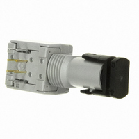
Manufacturer Part Number
HFBR-1414TZ
Description
XMITTER FIBER OPTIC HIGH PWR ST
Manufacturer
Avago Technologies US Inc.
Specifications of HFBR-1414TZ
Wavelength
820nm
Voltage - Forward (vf) Typ
1.7V
Current - Dc Forward (if)
100mA
Voltage - Dc Reverse (vr) (max)
1.8V
Capacitance
55pF
Connector Type
ST
Function
High performance fiber optic communication links for information systems and industrial applications.
Product
Transmitter
Data Rate
160 MBd
Diode Capacitance
55 pF
Maximum Rise Time
6.5 ns
Maximum Fall Time
6.5 ns
Pulse Width Distortion
7.56 ns
Operating Supply Voltage
7 VDC
Maximum Operating Temperature
+ 85 C
Minimum Operating Temperature
- 40 C
Lead Free Status / RoHS Status
Lead free / RoHS Compliant
Spectral Bandwidth
-
Lead Free Status / Rohs Status
Lead free / RoHS Compliant
For Use With
Multimode Glass, Hard Clad Silica
Lead Free Status / RoHS Status
Lead free / RoHS Compliant, Lead free / RoHS Compliant
Other names
516-2039
Available stocks
Company
Part Number
Manufacturer
Quantity
Price
Company:

Part Number:
HFBR-1414TZ
Manufacturer:
TI
Quantity:
5 560
Company:
Part Number:
HFBR-1414TZ
Manufacturer:
Avago Technologies US Inc.
Quantity:
1 871
Part Number:
HFBR-1414TZ
Manufacturer:
AVAGO/安华高
Quantity:
20 000


HFBR-24x2Z Low-Cost 5 MBd Receiver
Description
The HFBR-24x2Z fiber optic receiver is designed to
operate with the Avago Technologies HFBR-14xxZ fiber
optic transmitter and 50/125 µm, 62.5/125 µm, 100/
140 µm, and 200 µm HCS® fiber optic cable. Consistent
coupling into the receiver is assured by the lensed
optical system (Figure 1). Response does not vary with
fiber size ≤ 0.100 µm.
The HFBR-24x2Z receiver incorporates an integrated
photo IC containing a photodetector and dc amplifier
driving an opencollector Schottky output transistor.
The HFBR-24x2Z is designed for direct interfacing to
popular logic families. The absence of an internal pull-
up resistor allows the open-collector output to be used
with logic families such as CMOS requiring voltage
excursions much higher than V
Both the open-collector “Data” output Pin 6 and V
Pin 2 are referenced to “Com” Pin 3, 7. The “Data”
output allows busing, strobing and wired “OR” circuit
configurations. The transmitter is designed to operate
from a single +5 V supply. It is essential that a bypass
capacitor (0.1 mF ceramic) be connected from Pin 2
(V
Absolute Maximum Ratings
20
Parameter
Storage Temperature
Operating
Lead Soldering Cycle
Supply Voltage
Output Current
Output Voltage
Output Collector
Power Dissipation
Fan Out (TTL)
Temperature
CC
Temp
Time
) to Pin 3 (circuit common) of the receiver.
Symbol
I
P
N
T
T
V
V
O
S
A
O AV
CC
O
CC
.
Min
-55
-40
-0.5
-0.5
CC
Max
+85
+85
+260
10
7.0
25
18.0
5
40
Housed Product
Unhoused Product
NOTES:
1. PINS 1, 4, 5 AND 8 ARE ELECTRICALLY CONNECTED
2. PINS 3 AND 7 ARE ELECTRICALLY CONNECTED TO HEADER
BOTTOM VIEW
BOTTOM VIEW
1
4
PIN
1
3
4
5
7
8
2
6
1
2
1
1
2
1
2
3
FUNCTION
NC
V
COMMON
NC
NC
DATA
COMMON
NC
4 5
3
2
1
CC
(5 V)
6
7
8
PIN 1 INDICATOR
2
6
7 & 3
V
DATA
COMMON
PIN
1
2
3
4
Units
°C
°C
°C
sec
V
mA
V
mW
cc
FUNCTION
V
COMMON
DATA
COMMON
CC
(5 V)
Reference
Note 1
Note 2
Related parts for HFBR-1414TZ
Image
Part Number
Description
Manufacturer
Datasheet
Request
R

Part Number:
Description:
FIBER OPTIC CBL SIMPLEX 1=100M
Manufacturer:
Avago Technologies US Inc.
Datasheet:

Part Number:
Description:
FIBER OPTIC CBL SIMPLEX 1=500M
Manufacturer:
Avago Technologies US Inc.
Datasheet:

Part Number:
Description:
FIBER OPTIC CONN LATCH GRY SIMPL
Manufacturer:
Avago Technologies US Inc.
Datasheet:

Part Number:
Description:
FIBER OPTIC CONN LATCH BLU SIMPL
Manufacturer:
Avago Technologies US Inc.
Datasheet:

Part Number:
Description:
XMITTER VERSATILE LINK HORZ
Manufacturer:
Avago Technologies US Inc.
Datasheet:

Part Number:
Description:
Fiber Optic Transmitters, Receivers, Transceivers 1300nm 155MBd 16-pin DIP ST Rx
Manufacturer:
Avago Technologies US Inc.

Part Number:
Description:
FIBER OPTIC CBL DUPLEX 1=100M
Manufacturer:
Avago Technologies US Inc.
Datasheet:
Part Number:
Description:
FIBER OPTIC CBL SIMPLEX 1=500M
Manufacturer:
Avago Technologies US Inc.
Datasheet:
Part Number:
Description:
FIBER OPTIC CBL DUPLEX 1=500M
Manufacturer:
Avago Technologies US Inc.
Datasheet:

Part Number:
Description:
FIBER OPTIC CBL SIMPLEX 1=100M
Manufacturer:
Avago Technologies US Inc.
Datasheet:

Part Number:
Description:
OPTOCOUPLER GATE DRV 2A 16-SOIC
Manufacturer:
Avago Technologies US Inc.
Datasheet:
Part Number:
Description:
OPTOCOUPLER 2CH 2.5A 16-SOIC
Manufacturer:
Avago Technologies US Inc.
Datasheet:

Part Number:
Description:
OPTOCOUPLER GATE DRV 0.4A 16SOIC
Manufacturer:
Avago Technologies US Inc.
Datasheet:

Part Number:
Description:
OPTOCOUPLER 2.0A 250KHZ 8-DIP
Manufacturer:
Avago Technologies US Inc.
Datasheet:

Part Number:
Description:
OPTOCOUPLER 2.0A 250KHZ GW 8-SMD
Manufacturer:
Avago Technologies US Inc.
Datasheet: