SOIC8EV Microchip Technology, SOIC8EV Datasheet - Page 16
SOIC8EV
Manufacturer Part Number
SOIC8EV
Description
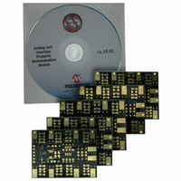
BOARD DEMO 8SOIC/MSOP/TSSOP/DIP
Manufacturer
Microchip Technology
Specifications of SOIC8EV
Mfg Application Notes
Interface Product Design Guide
Main Purpose
Bare Evaluation Board
Embedded
No
Primary Attributes
8- Pin SOIC/DIP/TSSOP/MSOP Evaluation Board
Secondary Attributes
For PICmicro® MCUs, ADCs, DACs and other Devices
Lead Free Status / RoHS Status
Lead free / RoHS Compliant
Utilized Ic / Part
-
Lead Free Status / Rohs Status
Lead free / RoHS Compliant
Available stocks
Company
Part Number
Manufacturer
Quantity
Price
Company:

Part Number:
SOIC8EV
Manufacturer:
Microchip Technology
Quantity:
135


8-Pin SOIC/MSOP/TSSOP/DIP Evaluation Board User’s Guide
2.4
DS51544A-page 12
8-PIN SOIC/MSOP/TSSOP/DIP EVALUATION BOARD DESCRIPTION
The 8-Pin SOIC/MSOP/TSSOP/DIP Evaluation Board PCB is designed to be flexible
in the type of device evaluation that can be implemented.
The following sections describe each element of this evaluation board in further detail.
Refer to Figure 2-3.
2.4.1
The 8-Pin SOIC/MSOP/TSSOP/DIP Evaluation Board has a VDD Pad and a VSS pad.
These pads can have connection posts installed that allows easy connection to the
power (V
surface-mount connectors.
The power and ground planes are connected to the appropriate passive components
on the PCB (such as power plane to R2X and ground plane to R3X and C1X).
2.4.2
For each package pin (pins 1 to 8), there is a PCB pad (pads 1 to 8). The device will
have some power pins (V
PCB, vias to the power and ground plane have been installed close to each PCB pad.
This allows any pad to be connected to the power or ground plane, so when power is
connected to the VDD and VSS pads, the power is connected to the appropriate device
pin.
FIGURE 2-3:
Revision 1 of this PCB has an issue that these vias are not connected to the desired
power and ground planes (they are open). For additional information, refer to
Appendix D. “Rev. 1 PCB Errata”.
Jumpering to VSS
DD
Power and Ground
PCB PADs
) and ground (V
Jumpering the PCB pad to either VDD or VSS.
DD
SS
) and some ground pins (V
) planes. The layout allows either through-hole or
Jumpering to VDD
SS
). To ease connections on the
© 2005 Microchip Technology Inc.
Related parts for SOIC8EV
Image
Part Number
Description
Manufacturer
Datasheet
Request
R

Part Number:
Description:
SOIC-8
Manufacturer:
Microchip Technology Inc.
Datasheet:
Part Number:
Description:
SOIC-8
Manufacturer:
Microchip Technology Inc.
Datasheet:
Part Number:
Description:
SOIC
Manufacturer:
Microchip Technology Inc.
Datasheet:
Part Number:
Description:
SOIC-8-TR/256K, 32K X 8, 2.5V SER EE, IND
Manufacturer:
Microchip Technology Inc.
Part Number:
Description:
SOIC 8/150STAND ALONE LIN TRANSCEIVER
Manufacturer:
Microchip Technology Inc.
Datasheet:
Part Number:
Description:
SOIC 20/USB TO SPI PROTOCOL CONVERTER
Manufacturer:
Microchip Technology Inc.
Datasheet:
Part Number:
Description:
SOIC 8/I�/1.5KB OTP, 41 RAM, 6 I/O
Manufacturer:
Microchip Technology Inc.
Part Number:
Description:
soic 8/I�/8-Pin, Flash-Based 8-Bit CMOS Microcontrollers
Manufacturer:
Microchip Technology Inc.
Part Number:
Description:
SOIC/I�/Microcontroller Series EPROM/ROM-Based 8-bit CMOS
Manufacturer:
Microchip Technology Inc.
Part Number:
Description:
SOIC 8/C�/8 Mbit SPI Serial Flash 50MHZ
Manufacturer:
Microchip Technology Inc.
Datasheet:
Part Number:
Description:
Manufacturer:
Microchip Technology Inc.
Datasheet:
Part Number:
Description:
Manufacturer:
Microchip Technology Inc.
Datasheet:
Part Number:
Description:
Manufacturer:
Microchip Technology Inc.
Datasheet: