MCP3909EV-MCU16 Microchip Technology, MCP3909EV-MCU16 Datasheet - Page 15
MCP3909EV-MCU16
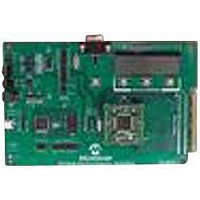
Manufacturer Part Number
MCP3909EV-MCU16
Description
EVALUATION BOARD FOR MCP3909
Manufacturer
Microchip Technology
Datasheets
1.MCP3909T-ISS.pdf
(44 pages)
2.MCP3909T-ISS.pdf
(104 pages)
3.MCP3909EV-MCU16.pdf
(38 pages)
Specifications of MCP3909EV-MCU16
Number Of Adc's
2
Number Of Bits
16
Sampling Rate (per Second)
15k
Data Interface
Serial
Inputs Per Adc
1 Differential
Input Range
±1 V
Voltage Supply Source
Analog and Digital
Operating Temperature
-40°C ~ 85°C
Utilized Ic / Part
MCP3909
Silicon Manufacturer
Microchip
Application Sub Type
ADC
Kit Application Type
Data Converter
Silicon Core Number
MCP3909
Kit Contents
Board
Lead Free Status / RoHS Status
Lead free / RoHS Compliant


3.0
The descriptions of the pins are listed in
TABLE 3-1:
3.1
DV
within the MCP3909.
This pin requires appropriate bypass capacitors and
should be maintained to 5V ±10% for specified
operation.
Information”.
3.2
HPF controls the state of the high-pass filter in both
input channels. A logic ‘1’ enables both filters,
removing any DC offset coming from the system or the
device. A logic ‘0’ disables both filters allowing DC
voltages to be measured.
© 2009 Microchip Technology Inc.
DD
MCP3909
is the power supply pin for the digital circuitry
SSOP
PIN DESCRIPTIONS
Digital V
High-Pass Filter Input Logic Pin
(HPF)
10
11
12
13
14
15
16
17
18
19
20
21
22
23
24
1
2
3
4
5
6
7
8
9
Refer
PIN FUNCTION TABLE
DD
to
(DV
REFIN/OUT
SDO / NEG
Section 6.0
SCK / F2
SDI / F1
Symbol
CS / F0
HF
MCLR
OSC1
OSC2
F
F
CH0+
CH1+
DV
A
D
AV
CH0-
CH1-
HPF
DD
OUT1
OUT0
NC
NC
G1
G0
GND
GND
OUT
DD
DD
)
“Applications
Table
Digital Power Supply Pin
High-Pass Filters Control Logic Pin
Analog Power Supply Pin
No Connect
Master Clear Logic Input Pin
Analog Ground Pin, Return Path for internal analog circuitry
Serial Clock or Frequency Control for HF
Serial Data Input or Frequency Control for F
Chip Select or Frequency Control for F
Gain Control Logic Input Pin
Gain Control Logic Input Pin
Oscillator Crystal Connection Pin or Clock Input Pin
Oscillator Crystal Connection Pin or Clock Output Pin
No Connect
Serial Data Out or Negative Power Logic Output Pin
Digital Ground Pin, Return Path for Internal Digital Circuitry
High-Frequency Logic Output Pin (Intended for Calibration)
Differential Mechanical Counter Logic Output Pin
Differential Mechanical Counter Logic Output Pin
Non-Inverting Analog Input Pin for Channel 0 (Current Channel)
Inverting Analog Input Pin for Channel 0 (Current Channel)
Inverting Analog Input Pin for Channel 1 (Voltage Channel)
Non-Inverting Analog Input Pin for Channel 1 (Voltage Channel)
Voltage Reference Input/Output Pin
3-1.
3.3
AV
within the MCP3909.
This pin requires appropriate bypass capacitors and
should be maintained to 5V ±10% for specified
operation.
Information”.
DD
is the power supply pin for the analog circuitry
Analog V
Description
Refer
OUT0/1
OUT
to
OUT0/1
DD
Logic Input Pin
Logic Input Pin
(AV
Section 6.0
Logic Input Pin
DD
MCP3909
)
DS22025B-page 15
“Applications
Related parts for MCP3909EV-MCU16
Image
Part Number
Description
Manufacturer
Datasheet
Request
R

Part Number:
Description:
Manufacturer:
Microchip Technology Inc.
Datasheet:
Part Number:
Description:
Manufacturer:
Microchip Technology Inc.
Datasheet:
Part Number:
Description:
Manufacturer:
Microchip Technology Inc.
Datasheet:
Part Number:
Description:
Manufacturer:
Microchip Technology Inc.
Datasheet:
Part Number:
Description:
Manufacturer:
Microchip Technology Inc.
Datasheet:
Part Number:
Description:
Manufacturer:
Microchip Technology Inc.
Datasheet:
Part Number:
Description:
Manufacturer:
Microchip Technology Inc.
Datasheet:
Part Number:
Description:
Manufacturer:
Microchip Technology Inc.
Datasheet: