MCP355XDV-MS1 Microchip Technology, MCP355XDV-MS1 Datasheet - Page 11
MCP355XDV-MS1
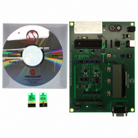
Manufacturer Part Number
MCP355XDV-MS1
Description
BOARD DEV SENSOR APP MCP355X
Manufacturer
Microchip Technology
Datasheets
1.MCP3553-ESN.pdf
(36 pages)
2.MCP355XDV-MS1.pdf
(36 pages)
3.MCP3551DM-PCTL.pdf
(30 pages)
Specifications of MCP355XDV-MS1
Number Of Adc's
1
Number Of Bits
22
Data Interface
Serial
Inputs Per Adc
1 Differential
Input Range
±0.3 V
Voltage Supply Source
Single Supply
Operating Temperature
-40°C ~ 125°C
Utilized Ic / Part
MCP355x
Processor To Be Evaluated
MCP355x
Interface Type
RS-232, USB
Lead Free Status / RoHS Status
Not applicable / Not applicable
Lead Free Status / RoHS Status
Lead free / RoHS Compliant, Not applicable / Not applicable
Available stocks
Company
Part Number
Manufacturer
Quantity
Price
Company:

Part Number:
MCP355XDV-MS1
Manufacturer:
MICROCHIP
Quantity:
12 000


3.0
TABLE 3-1:
3.1
The MCP3550/1/3 devices accept single-ended refer-
ence voltages from 0.1V to V
output noise is dominated by thermal noise, which is
independent of the reference voltage, the output noise
is not significantly improved by diminishing the refer-
ence voltage at the V
reference will significantly improve the INL perfor-
mance (see Figure 2-4); the INL max error is
proportional to V
3.2
The MCP3550/1/3 devices accept a fully differential
analog input voltage to be connected on the V
V
verted is defined by V
voltage range specified for ensured accuracy is from
-V
valid and usable codes with the inputs overranged by
up to 12% (see Section 5.0 “Serial Interface”) at
room temperature. This overrange is clearly specified
by two overload bits in the output code.
The absolute voltage range on these input pins extends
from V
below this range will create leakage currents through
the Electrostatic Discharge (ESD) diodes. This current
will increase exponentially, degrading the accuracy and
noise performance of the device. The common mode of
the analog inputs should be chosen such that both the
differential analog input range and the absolute voltage
range on each pin are within the specified operating
range defined in Section 1.0 “Electrical Characteris-
tics”.
3.3
V
circuitry within the MCP3550/1/3. This pin requires an
appropriate bypass capacitor of 0.1 µF. The voltage on
© 2007 Microchip Technology Inc.
Type Identification: I = Input; O = Output; P = Power
IN
DD
REF
- input pins. The differential voltage that is con-
is the power supply pin for the analog and digital
to +V
Pin No.
SS
PIN DESCRIPTIONS
Voltage Reference (V
Analog Inputs (V
Supply Voltage (V
– 0.3V to V
1
2
3
4
5
6
7
8
REF
. However, the converter will still output
REF
PIN FUNCTION TABLE
2
.
REF
DD
IN
= V
+ 0.3V. Any voltage above or
SDO/RDY
input pin. A reduced voltage
Symbol
V
IN
V
SCK
V
V
V
CS
REF
IN
+ – V
IN
DD
SS
DD
IN
+
-
DD
. Since the converter
+, V
IN
, V
REF
-. The differential
IN
SS
-)
)
)
I/O/P
IN
O
P
P
+ and
I
I
I
I
I
Reference Voltage Analog Input Pin
Non-inverting Analog Input Pin
Inverting Analog Input Pin
Ground Pin
Serial Clock Digital Input Pin
Data/Ready Digital Output Pin
Chip Select Digital Input Pin
Positive Supply Voltage Pin
this pin should be maintained in the 2.7V to 5.5V range
for specified operation. V
current return path for both analog and digital circuitry
of the MCP3550/1/3. If an analog ground plane is
available, it is recommended that this device be tied to
the analog ground plane of the Printed Circuit Board
(PCB).
3.4
SCK synchronizes data communication with the
device. The device operates in both SPI mode 1,1 and
SPI mode 0,0. Data is shifted out of the device on the
falling edge of SCK. Data is latched in on the rising
edge of SCK. During CS high times, the SCK pin can
idle either high or low.
3.5
SDO/RDY is the output data pin for the device. Once a
conversion is complete, this pin will go active-low,
acting as a ready flag. Subsequent falling clock edges
will then place the 24-bit data word (two overflow bits
and 22 bits of data, see Section 5.0 “Serial Inter-
face”) on the SPI bus through the SDO pin. Data is
clocked out on the falling edge of SCK.
3.6
CS gates all communication to the device and can be
used to select multiple devices that share the same
SCK and SDO/RDY pins. This pin is also used to
control the internal conversions, which begin on the
falling edge of CS. Raising CS before the first internal
conversion is complete places the device in Single
Conversion mode. Leaving CS low will place the
device in Continuous Conversion mode (i.e., additional
internal conversions will automatically occur). CS may
be tied permanently low for two-wire Continuous
Conversion mode operation. SDO/RDY enters a high-
impedance state with CS high.
Serial Clock (SCK)
Data Output (SDO/RDY)
Chip Select (CS)
Function
MCP3550/1/3
SS
is the ground pin and the
DS21950D-page 11
Related parts for MCP355XDV-MS1
Image
Part Number
Description
Manufacturer
Datasheet
Request
R

Part Number:
Description:
Manufacturer:
Microchip Technology Inc.
Datasheet:
Part Number:
Description:
Manufacturer:
Microchip Technology Inc.
Datasheet:
Part Number:
Description:
Manufacturer:
Microchip Technology Inc.
Datasheet:
Part Number:
Description:
Manufacturer:
Microchip Technology Inc.
Datasheet:
Part Number:
Description:
Manufacturer:
Microchip Technology Inc.
Datasheet:
Part Number:
Description:
Manufacturer:
Microchip Technology Inc.
Datasheet:
Part Number:
Description:
Manufacturer:
Microchip Technology Inc.
Datasheet:
Part Number:
Description:
Manufacturer:
Microchip Technology Inc.
Datasheet: