MCP355XDV-MS1 Microchip Technology, MCP355XDV-MS1 Datasheet - Page 17
MCP355XDV-MS1
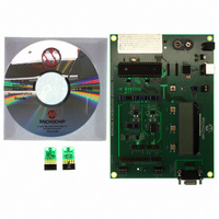
Manufacturer Part Number
MCP355XDV-MS1
Description
BOARD DEV SENSOR APP MCP355X
Manufacturer
Microchip Technology
Datasheets
1.MCP3553-ESN.pdf
(36 pages)
2.MCP355XDV-MS1.pdf
(36 pages)
3.MCP3551DM-PCTL.pdf
(30 pages)
Specifications of MCP355XDV-MS1
Number Of Adc's
1
Number Of Bits
22
Data Interface
Serial
Inputs Per Adc
1 Differential
Input Range
±0.3 V
Voltage Supply Source
Single Supply
Operating Temperature
-40°C ~ 125°C
Utilized Ic / Part
MCP355x
Processor To Be Evaluated
MCP355x
Interface Type
RS-232, USB
Lead Free Status / RoHS Status
Not applicable / Not applicable
Lead Free Status / RoHS Status
Lead free / RoHS Compliant, Not applicable / Not applicable
Available stocks
Company
Part Number
Manufacturer
Quantity
Price
Company:

Part Number:
MCP355XDV-MS1
Manufacturer:
MICROCHIP
Quantity:
12 000


5.0
5.1
Serial communication between the microcontroller and
the MCP3550/1/3 devices is achieved using CS, SCK
and SDO/RDY. There are two modes of operation:
Single Conversion and Continuous Conversion. CS
controls the conversion start. There are 24 bits in the
data word: 22 bits of conversion data and two overflow
bits. The conversion process takes place via the inter-
nal oscillator and the status of this conversion must be
detected. The typical method of communication is
shown in Figure 5-1. The status of the internal conver-
sion is the SDO/RDY pin and is available with CS low.
A High state on SDO/RDY means the device is busy
converting, while a Low state means the conversion is
finished and data is ready for transfer using SCK.
SDO/RDY remains in a high-impedance state when
CS is held high. CS must be low when clocking out the
data using SCK and SDO/RDY.
Bit 22 is Overflow High (OVH) when V
OVH toggles to logic ‘1’, detecting an overflow high in
the analog input voltage.
Bit 23 is Overflow Low (OVL) when V
toggles to logic ‘1’, detecting an overflow low in the
analog input voltage. The state OVH = OVL = ‘1’ is not
defined and should be considered as an interrupt for
the SPI interface meaning erroneous communication.
FIGURE 5-1:
Analog Input Voltages.
© 2007 Microchip Technology Inc.
SDO/RDY
SCK
CS
SERIAL INTERFACE
Overview
READY
Typical Serial Device Communication and Example Digital Output Codes for Specific
D
R
O O
L
IN
H
IN
21 20 19 18 17
> V
< -V
REF
REF
– 1 LSB,
, OVL
16
15 14 13 12 11 10 9
Bit 21 to bit 0 represents the output code in 22-bit
binary two's complement. Bit 21 is the sign bit and is
logic ‘0’ when the differential analog input is positive
and logic ‘1’ when the differential analog input is
negative. From Bit 20 to bit 0, the output code is given
MSb first (MSb is bit 20 and LSB is Bit 0). When the
analog input value is comprised between -V
V
The relationship between input voltage and output
code is shown in Figure 5-1.
The delta-sigma modulator saturation point for the
differential analog input is located at around ±112% of
V
tor will still give accurate output codes with an over-
range of 12% below or above the reference voltage.
Unlike the usual 22-bit device, the 22-bit output code
will not lock at 0x1FFFFF for positive sign inputs or
0x200000 for negative sign inputs in order to take
advantage of the overrange capabilities of the device.
This can be practical for closed-loop operations, for
instance. In case of an overflow, the output code
becomes a 23-bit two's complement output code,
where the sign bit will be the OVL bit. If an overflow high
or low is detected, OVL (bit 23) becomes the sign bit
(instead of bit 21), the MSb is then bit 21 and the con-
verter can be used as a 23-bit two's complement code
converter, with output code from bits B21 to B0, and
OVL as the sign bit. Figure 5-1 summarizes the output
coding data format with or without overflow high and
low.
REF
REF
– 1 LSB, the two overflow bits are set to logic ‘0’.
(at room temperature), meaning that the modula-
8
MCP3550/1/3
7 6 5 4 3 2 1
DS21950D-page 17
0
REF
HI-Z
and
Related parts for MCP355XDV-MS1
Image
Part Number
Description
Manufacturer
Datasheet
Request
R

Part Number:
Description:
Manufacturer:
Microchip Technology Inc.
Datasheet:
Part Number:
Description:
Manufacturer:
Microchip Technology Inc.
Datasheet:
Part Number:
Description:
Manufacturer:
Microchip Technology Inc.
Datasheet:
Part Number:
Description:
Manufacturer:
Microchip Technology Inc.
Datasheet:
Part Number:
Description:
Manufacturer:
Microchip Technology Inc.
Datasheet:
Part Number:
Description:
Manufacturer:
Microchip Technology Inc.
Datasheet:
Part Number:
Description:
Manufacturer:
Microchip Technology Inc.
Datasheet:
Part Number:
Description:
Manufacturer:
Microchip Technology Inc.
Datasheet: