MCP355XDV-MS1 Microchip Technology, MCP355XDV-MS1 Datasheet - Page 15
MCP355XDV-MS1
Manufacturer Part Number
MCP355XDV-MS1
Description
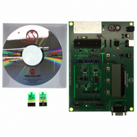
BOARD DEV SENSOR APP MCP355X
Manufacturer
Microchip Technology
Datasheets
1.MCP3553-ESN.pdf
(36 pages)
2.MCP355XDV-MS1.pdf
(36 pages)
3.MCP3551DM-PCTL.pdf
(30 pages)
Specifications of MCP355XDV-MS1
Number Of Adc's
1
Number Of Bits
22
Data Interface
Serial
Inputs Per Adc
1 Differential
Input Range
±0.3 V
Voltage Supply Source
Single Supply
Operating Temperature
-40°C ~ 125°C
Utilized Ic / Part
MCP355x
Processor To Be Evaluated
MCP355x
Interface Type
RS-232, USB
Lead Free Status / RoHS Status
Not applicable / Not applicable
Lead Free Status / RoHS Status
Lead free / RoHS Compliant, Not applicable / Not applicable
Available stocks
Company
Part Number
Manufacturer
Quantity
Price
Company:

Part Number:
MCP355XDV-MS1
Manufacturer:
MICROCHIP
Quantity:
12 000


4.4
The MCP3550/1/3 devices accept a fully differential
analog input voltage to be connected to the V
V
is defined by V
range specified for ensured accuracy is from -V
+V
The converter will output valid and usable codes from -
112% to 112% of output range (see Section 5.0
“Serial Interface”) at room temperature. The ±12%
overrange is clearly specified by two overload bits in
the output code: OVH and OVL. This feature allows for
system calibration of a positive gain error.
The absolute voltage range on these input pins extends
from V
above or below this range, the leakage currents of the
ESD diodes will increase exponentially, degrading the
accuracy and noise performance of the converter. The
common mode of the analog inputs should be chosen
such that both the differential analog input range and
absolute voltage range on each pin are within the
specified operating range defined in Section 1.0
“Electrical Characteristics”.
Both the analog differential inputs and the reference
input have switched-capacitor input structures. The
input capacitors are charged and discharged alterna-
tively with the input and the reference in order to
process a conversion. The charge and discharge of the
input capacitors create dynamic input currents at the
V
sampling capacitor. This current is a function of the
differential input voltages and their respective common
modes. The typical value of the differential input imped-
ance is 2.4 MΩ, with V
DC leakage current caused by the ESD input diodes,
even though on the order of 1 nA, can cause additional
offset errors proportional to the source resistance at the
V
From a transient response standpoint and as a first-
order approximation, these input structures form a
simple RC filtering circuit with the source impedance in
series with the R
of the input switch and the sampling capacitor. In order
to ensure the accuracy of the sampled charge, proper
settling time of the input circuit has to be considered.
Slow settling of the input circuit will create additional
gain error. As a rule of thumb, in order to obtain 1 ppm
absolute measurement accuracy, the sampling period
must be 14 times greater than the input circuit RC time
constant.
© 2007 Microchip Technology Inc.
IN-
IN
IN
REF
+ and V
+ and V
input pins. The differential voltage that is converted
.
SS
Differential Analog Inputs
- 0.3V to V
IN
IN
- input pins.
- input pins inversely proportional to the
IN
ON
= V
(switched resistance when closed)
DD
IN
CM
+ – V
+ 0.3V. If the input voltages are
= 2.5V, V
IN
-. The differential voltage
DD
= V
REF
= 5V. The
IN+
REF
and
to
4.5
The MCP3550/1/3 devices accept a single-ended
external reference voltage, to be connected on the
V
ADC is a differential voltage with the non-inverting input
connected to the V
connected to the V
voltage is V
reference is always (V
The MCP3550/1/3 devices accept a single-ended
reference voltage from 0.1V to V
output noise is dominated by thermal noise that is
independent of the reference voltage. Therefore, the
output noise is not significantly improved by lowering
the reference voltage at the V
reduced reference voltage will significantly improve the
INL performance since the INL max error is
proportional to V
The charge and discharge of the input capacitor create
dynamic input currents at the V
proportional to the sampling capacitor, which is a func-
tion of the input reference voltage. The typical value of
the single-ended input impedance is 2.4 MΩ, with
V
the ESD input diodes, though on the order of 1 nA
typically, can cause additional gain error proportional to
the source resistance at the V
4.6
The MCP3550/1/3 devices contain an internal Power-
On Reset (POR) circuit that monitors power supply
voltage V
correct device start-up at system power-up and power-
down events. The POR has built-in hysteresis and a
timer to give a high degree of immunity to potential
ripple and noise on the power supplies, as well as to
allow proper settling of the power supply during power-
up. A 0.1 µF decoupling capacitor should be mounted
as close as possible to the V
transient immunity.
The threshold voltage is set at 2.2V, with a tolerance of
approximately ±5%. If the supply voltage falls below
this threshold, the MCP3550/1/3 devices will be held in
a reset condition or in Shutdown mode. When the part
is in Shutdown mode, the power consumption is less
than 1 µA. The typical hysteresis value is around
200 mV in order to prevent reset during brown-out or
other glitches on the power supply.
REF
DD
= V
input pin. Internally, the reference voltage for the
REF
Voltage Reference Input Pin
Power-On Reset (POR)
DD
REF
= 5V. The DC leakage current caused by
during operation. This circuit ensures
REF
- V
SS
SS
2
MCP3550/1/3
REF
(see Figure 2-4).
REF
pin. The value of the reference
and the common mode of the
pin and the inverting input
- V
DD
SS
REF
REF
pin, providing additional
)/2.
REF
input pin. However, a
pin.
DD.
input pin inversely
DS21950D-page 15
The converter
Related parts for MCP355XDV-MS1
Image
Part Number
Description
Manufacturer
Datasheet
Request
R

Part Number:
Description:
Manufacturer:
Microchip Technology Inc.
Datasheet:
Part Number:
Description:
Manufacturer:
Microchip Technology Inc.
Datasheet:
Part Number:
Description:
Manufacturer:
Microchip Technology Inc.
Datasheet:
Part Number:
Description:
Manufacturer:
Microchip Technology Inc.
Datasheet:
Part Number:
Description:
Manufacturer:
Microchip Technology Inc.
Datasheet:
Part Number:
Description:
Manufacturer:
Microchip Technology Inc.
Datasheet:
Part Number:
Description:
Manufacturer:
Microchip Technology Inc.
Datasheet:
Part Number:
Description:
Manufacturer:
Microchip Technology Inc.
Datasheet: