KDC5514-Q48EVAL Intersil, KDC5514-Q48EVAL Datasheet
KDC5514-Q48EVAL
Specifications of KDC5514-Q48EVAL


Related parts for KDC5514-Q48EVAL

KDC5514-Q48EVAL Summary of contents
Page 1
... CAUTION: These devices are sensitive to electrostatic discharge; follow proper IC Handling Procedures. | 1-888-INTERSIL or 1-888-468-3774 Intersil (and design registered trademark of Intersil Americas Inc. FemtoCharge is a trademark of Kenet Inc. Copyright Intersil Americas Inc. 2008, 2009. All Rights Reserved All other trademarks mentioned are the property of their respective owners. KAD5514P FN6804.2 ...
Page 2
... These Intersil Pb-free plastic packaged products employ special Pb-free material sets, molding compounds/die attach materials, and 100% matte tin plate plus anneal (e3 termination finish, which is RoHS compliant and compatible with both SnPb and Pb-free soldering operations). Intersil Pb-free products are MSL classified at Pb-free peak reflow temperatures that meet or exceed the Pb-free requirements of IPC/JEDEC J STD- 020 ...
Page 3
Table of Contents Pin-Compatible Family...................................................... 1 Key Specifications ............................................................ 1 Electrical Specifications ....................................................4 Digital Specifications ........................................................ 6 Timing Diagrams ............................................................... 7 Switching Specifications .................................................. 8 Pinout/Package Information............................................. 9 Pin Descriptions - 72QFN ................................................ 9 Pin Descriptions - 48QFN .............................................. 12 ...
Page 4
Absolute Maximum Ratings AVDD to AVSS -0.4V to 2.1V OVDD ...
Page 5
Electrical Specifications All specifications apply under the following conditions unless otherwise noted: AVDD = 1.8V, OVDD = 1.8V -40°C to +85°C (typical specifications at +25°C (per speed grade). (Continued) PARAMETER SYMBOL CONDITIONS Total Power Dissipation Normal ...
Page 6
Electrical Specifications All specifications apply under the following conditions unless otherwise noted: AVDD = 1.8V, OVDD = 1.8V -40°C to +85°C (typical specifications at +25°C (per speed grade). (Continued) PARAMETER SYMBOL CONDITIONS Intermodulation IMD f = ...
Page 7
Timing Diagrams SAMPLE N INP INN t A CLKN CLKP t CPD LATENCY = L CYCLES CLKOUTN CLKOUTP D[12/10/8/6/4/2/0]P PD ODD BITS EVEN BITS ODD BITS EVEN BITS N-L N D[12/10/8/6/4/2/0]N ...
Page 8
Switching Specifications PARAMETER ADC OUTPUT Aperture Delay RMS Aperture Jitter Output Clock to Data DDR, Rising Edge Propagation Delay, LVDS Mode DDR, Falling Edge (Note 9) SDR, Falling Edge Output Clock to Data DDR, Rising Edge Propagation Delay, CMOS Mode ...
Page 9
Pinout/Package Information Pin Descriptions - 72QFN PIN NUMBER LVDS [LVCMOS] NAME 1, 6, 12, 19, 24, 71 AVDD 2-5, 13, 14, 17, 18 DNC 7, 8, 11, 72 AVSS 9, 10 VINN, VINP 15 VCM 16 CLKDIV 20, 21 CLKP, ...
Page 10
Pin Descriptions - 72QFN PIN NUMBER LVDS [LVCMOS] NAME 46 RLVDS 47 CLKOUTN [NC] 48 CLKOUTP [CLKOUT] 49 D8N [NC] 50 D8P [D8] 51 D9N [NC] 52 D9P [D9] 53 D10N [NC] 54 D10P [D10] 57 D11N [NC] 58 D11P ...
Page 11
Pinout 72 71 AVDD 1 DNC 2 DNC 3 4 DNC 5 DNC 6 AVDD 7 AVSS 8 AVSS 9 VINN 10 VINP 11 AVSS 12 AVDD 13 DNC 14 DNC 15 VCM 16 CLKDIV 17 DNC DNC 18 19 ...
Page 12
Pin Descriptions—48QFN PIN NUMBER 1, 9, 13, 17 19, 29 ...
Page 13
Pin Descriptions—48QFN PIN NUMBER Exposed Paddle NOTE: LVCMOS Output Mode Functionality is shown in brackets ( Connection) Pinout 1 AVDD 2 DNC 3 DNC 4 DNC AVSS 5 6 VINN 7 VINP 8 ...
Page 14
Typical Performance Curves 90 SFDR @ 125MSPS SFDR @ 125MSPS SNR @ 125MSPS SNR @ 125MSPS 70 65 SNR @ 250MSPS SNR @ 250MSPS 60 55 SFDR @ 250MSPS SFDR @ 250MSPS 50 0M 200M 400M INPUT ...
Page 15
Typical Performance Curves 500 450 400 SDR 350 300 250 200 150 100 100 130 SAMPLE RATE (MSPS) FIGURE 11. POWER vs f SAMPLE 2048 4096 6144 8192 ...
Page 16
Typical Performance Curves 0 AIN = -1.0dBFS SNR = 69.1dBFS -20 SFDR = 82.7dBc SINAD = 68.9dBFS -40 -60 -80 -100 -120 0M 20M 40M 60M FREQUENCY (Hz) FIGURE 17. SINGLE-TONE SPECTRUM @ 105MHz 0 -20 -40 -60 -80 -100 ...
Page 17
Theory of Operation Functional Description The KAD5514P is based upon a 12-bit, 250MSPS A/D converter core that utilizes a pipelined successive approximation architecture (Figure 23). The input voltage is captured by a Sample-Hold Amplifier (SHA) and converted to a unit ...
Page 18
The calibration sequence is initiated on the rising edge of RESETN, as shown in Figure 24. The over-range output (OR) is set high once RESETN is pulled low, and remains in that state until calibration is complete. The OR output ...
Page 19
Analog Input A single fully differential input (VINP/VINN) connects to the sample and hold amplifier (SHA) of each unit ADC. The ideal full-scale input voltage is 1.45V, centered at the VCM voltage of 0.535V as shown in Figure 27. 1.8 ...
Page 20
TABLE 1. CLKDIV PIN SETTINGS CLKDIV PIN AVSS Float AVDD The clock divider can also be controlled through the SPI port, which overrides the CLKDIV pin setting. Details on this are contained in “Serial Peripheral Interface” on page 22. A ...
Page 21
Nap/Sleep Portions of the device may be shut down to save power during times when operation of the ADC is not required. Two power saving modes are available: Nap, and Sleep. Nap mode reduces power dissipation to less than 163mW ...
Page 22
GRAY CODE BINARY FIGURE 34. GRAY CODE TO BINARY CONVERSION Mapping of the input voltage to the various data formats is shown in Table 5. CSB SCLK SDIO R CSB SCLK SDIO ...
Page 23
SPI Physical Interface The serial clock pin (SCLK) provides synchronization for the data transfer. By default, all data is presented on the serial data input/output (SDIO) pin in three-wire mode. The state of the SDIO pin is set automatically in ...
Page 24
... ADDRESS 0X10: DEVICE_INDEX_A A common SPI map, which can accommodate single-channel or multi-channel devices, is used for all Intersil ADC products. Certain configuration commands (identified as Indexed in the SPI map) can be executed on a per-converter basis. This register determines which converter is being addressed for an Indexed command important to note that only a single converter can be addressed at a time ...
Page 25
The default value of each register will be the result of the self-calibration after initial power-up register incremented or decremented, the user should first read the register value then write the incremented or decremented value ...
Page 26
TABLE 11. CLOCK DIVIDER SELECTION VALUE CLOCK DIVIDER 000 001 010 100 ADDRESS 0X73: OUTPUT_MODE_A The output_mode_A register controls the physical output format of the data, as well as the logical coding. The KAD5514P can present output data in two ...
Page 27
TABLE 15. OUTPUT TEST MODES 0xC0[3:0] OUTPUT TEST VALUE MODE WORD 1 0000 Off 0001 Midscale 0010 Positive Full-Scale 0xFFFF 0011 Negative Full-Scale 0100 Checkerboard 0xAAAA 0101 Reserved 0110 Reserved 0111 One/Zero 0xFFFF 1000 User Pattern user_patt1 SPI Memory Map ...
Page 28
Addr Parameter Bit 7 (Hex) Name (MSB) 60-6F reserved 70 reserved 71 phase_slip 72 clock_divide 73 output_mode_A Output Mode [2:0] 000 = Pin Control 001 = LVDS 2mA 010 = LVDS 3mA 100 = LVCMOS other codes = reserved 74 ...
Page 29
Equivalent Circuits AVDD CSAMP 1.6pF INP Φ Φ 1000O Ω CSAMP AVDD 1.6pF INN Φ Φ FIGURE 43. ANALOG INPUTS AVDD AVDD Ω 75kO AVDD Ω 75kO 280O Ω INPUT Ω 75kO ...
Page 30
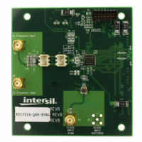
... Mode OUTFMT Data Coding ADC Evaluation Platform Intersil offers an ADC Evaluation platform which can be used to evaluate any of the KADxxxxx ADC family. The platform consists of a FPGA based data capture motherboard and a family of ADC daughtercards. This USB based platform allows a user to quickly evaluate the ADC’s performance at a user’ ...
Page 31
Definitions Analog Input Bandwidth is the analog input frequency at which the spectral output power at the fundamental frequency (as determined by FFT analysis) is reduced by 3dB from its full-scale low-frequency value. This is also referred to as Full ...
Page 32
... Accordingly, the reader is cautioned to verify that data sheets are current before placing orders. Information furnished by Intersil is believed to be accurate and reliable. However, no responsibility is assumed by Intersil or its subsidiaries for its use; nor for any infringements of patents or other rights of third parties which may result from its use ...
Page 33
Package Outline Drawing L48.7x7E 48 LEAD QUAD FLAT NO-LEAD PLASTIC PACKAGE Rev 1, 2/09 7.00 PIN 1 INDEX AREA 6 (4X) 0.15 TOP VIEW 6.80 Sq 5.60 Sq TYPICAL RECOMMENDED LAND PATTERN 33 KAD5514P Exp. DAP ...
Page 34
Package Outline Drawing L72.10x10D 72 LEAD QUAD FLAT NO-LEAD PLASTIC PACKAGE Rev 1, 11/08 10.00 PIN 1 INDEX AREA 6 (4X) 0.15 TOP VIEW 9.80 Sq 6.00 Sq TYPICAL RECOMMENDED LAND PATTERN 34 KAD5514P 10.00 37 ...