KDC5514-Q48EVAL Intersil, KDC5514-Q48EVAL Datasheet - Page 26
KDC5514-Q48EVAL
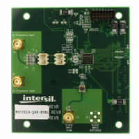
Manufacturer Part Number
KDC5514-Q48EVAL
Description
DAUGHTER CARD FOR KAD5514
Manufacturer
Intersil
Series
FemtoCharge™r
Datasheets
1.KAD5514P-25Q72.pdf
(34 pages)
2.KMB-001LEVALZ.pdf
(7 pages)
3.KDC5514EVALZ.pdf
(9 pages)
Specifications of KDC5514-Q48EVAL
Number Of Adc's
1
Number Of Bits
14
Sampling Rate (per Second)
250M
Data Interface
Parallel
Inputs Per Adc
1 Differential
Input Range
1.47 Vpp
Power (typ) @ Conditions
429mW @ 250MSPS
Voltage Supply Source
Single Supply
Operating Temperature
-40°C ~ 85°C
Utilized Ic / Part
KAD5514P-25, KMB001 Motherboard
For Use With
KMB001LEVAL - MOTHERBOARD FOR LVDS ADC CARD
Lead Free Status / RoHS Status
Lead free / RoHS Compliant


ADDRESS 0X73: OUTPUT_MODE_A
The output_mode_A register controls the physical output
format of the data, as well as the logical coding. The
KAD5514P can present output data in two physical formats:
LVDS or LVCMOS. Additionally, the drive strength in LVDS
mode can be set high (3mA) or low (2mA). By default, the
tri-level OUTMODE pin selects the mode and drive level (refer
to “Digital Outputs” on page 20). This functionality can be
overridden and controlled through the SPI, as shown in
Table 12.
Data can be coded in three possible formats: two’s
complement, Gray code or offset binary. By default, the
tri-level OUTFMT pin selects the data format (refer to “Data
Format” on page 21). This functionality can be overridden
and controlled through the SPI, as shown in Table 13.
This register is not changed by a Soft Reset.
ADDRESS 0X74: OUTPUT_MODE_B
ADDRESS 0X75: CONFIG_STATUS
Bit 6 DLL Range
This bit sets the DLL operating range to fast (default) or
slow.
VALUE
VALUE
VALUE
000
001
010
100
000
001
010
100
000
001
010
100
TABLE 11. CLOCK DIVIDER SELECTION
TABLE 13. OUTPUT FORMAT CONTROL
TABLE 12. OUTPUT MODE CONTROL
26
OUTPUT FORMAT
Two’s Complement
CLOCK DIVIDER
OUTPUT MODE
Offset Binary
Pin Control
Divide by 1
Divide by 2
Divide by 4
Pin Control
Gray Code
0x72[2:0]
Pin Control
LVDS 2mA
LVDS 3mA
0x93[2:0]
0x93[7:5]
LVCMOS
KAD5514P
Bit 4 DDR Enable
Internal clock signals are generated by a delay-locked loop
(DLL), which has a finite operating range. Table 14 shows
the allowable sample rate ranges for the slow and fast
settings.
The output_mode_B and config_status registers are used in
conjunction to enable DDR mode and select the frequency
range of the DLL clock generator. The method of setting
these options is different from the other registers.
The procedure for setting output_mode_B is shown in
Figure 42. Read the contents of output_mode_B and
config_status and XOR them. Then XOR this result with the
desired value for output_mode_B and write that XOR result
to the register.
Device Test
The KAD5514P can produce preset or user defined patterns
on the digital outputs to facilitate in-situ testing. A static word
can be placed on the output bus, or two different words can
alternate. In the alternate mode, the values defined as
Word 1 and Word 2 (as shown in Table 15) are set on the
output bus on alternating clock phases. The test mode is
enabled asynchronously to the sample clock, therefore
several sample clock cycles may elapse before the data is
present on the output bus.
ADDRESS 0XC0: TEST_IO
Bits 7:6 User Test Mode
The four LSBs in this register (Output Test Mode) determine
the test pattern in combination with registers 0xC2 through
0xC5. Refer to Table 16.
OUTPUT_MODE_B
CONFIG_STATUS
DLL RANGE
Setting this bit enables Double Data-Rate mode.
These bits set the test mode to static (0x00) or alternate
(0x01) mode. Other values are reserved.
FIGURE 42. SETTING OUTPUT_MODE_B REGISTER
Slow
Fast
READ
READ
0x74
0x75
TABLE 14. DLL RANGES
DESIRED
VALUE
MIN
40
80
f
S MAX
MAX
100
September 10, 2009
WRITE TO
MSPS
MSPS
UNIT
0x74
FN6804.2
Related parts for KDC5514-Q48EVAL
Image
Part Number
Description
Manufacturer
Datasheet
Request
R

Part Number:
Description:
Intersil Corporation [CMOS Serial Controller Interface]
Manufacturer:
Intersil Corporation
Datasheet:
Part Number:
Description:
Manufacturer:
Intersil Corporation
Datasheet:
Part Number:
Description:
357-036-542-201 CARDEDGE 36POS DL .156 BLK LOPRO
Manufacturer:
Intersil Corporation
Datasheet:
Part Number:
Description:
1024-Word x 4-Bit LSI Static RAM
Manufacturer:
Intersil Corporation
Datasheet:
Part Number:
Description:
General Purpose NPN Transistor Arrays FN341.4
Manufacturer:
Intersil Corporation
Datasheet:
Part Number:
Description:
CMOS 16-Bit Microprocessor
Manufacturer:
Intersil Corporation
Datasheet:
Part Number:
Description:
Manufacturer:
Intersil Corporation
Datasheet:
Part Number:
Description:
Manufacturer:
Intersil Corporation
Datasheet:
Part Number:
Description:
Manufacturer:
Intersil Corporation
Datasheet:
Part Number:
Description:
Manufacturer:
Intersil Corporation
Datasheet:
Part Number:
Description:
CMOS 6-Bit Latch and Decoder Memory Interfaces
Manufacturer:
Intersil Corporation
Datasheet:
Part Number:
Description:
CA3046General Purpose NPN Transistor Arrays
Manufacturer:
Intersil Corporation
Datasheet:
Part Number:
Description:
Manufacturer:
Intersil Corporation
Datasheet:
Part Number:
Description:
TR909 DLC/FLC SLIC with Low Power Standby
Manufacturer:
Intersil Corporation
Datasheet:
Part Number:
Description:
Manufacturer:
Intersil Corporation
Datasheet: