CDB5381 Cirrus Logic Inc, CDB5381 Datasheet
CDB5381
Specifications of CDB5381


Related parts for CDB5381


CDB5381 Summary of contents
Page 1
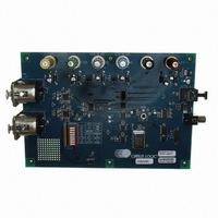
... The ADC uses a differential architecture which provides excellent noise rejection. The CS5381 is available in 24-pin TSSOP and SOIC packages for Commercial grade (-10° to +70° C). The CDB5381 Customer Demonstration board is also avail- able for device suggestions. Please refer to the on page 22 ...
Page 2
TABLE OF CONTENTS 1. PIN DESCRIPTIONS ............................................................................................................................... 4 2. CHARACTERISTICS AND SPECIFICATIONS....................................................................................... 5 SPECIFIED OPERATING CONDITIONS .................................................................................................... 5 ABSOLUTE MAXIMUM RATINGS............................................................................................................... 5 ANALOG CHARACTERISTICS (CS5381-KSZ/-KZZ).................................................................................. 6 DIGITAL FILTER CHARACTERISTICS....................................................................................................... 7 SWITCHING CHARACTERISTICS - SERIAL AUDIO PORT .................................................................... 10 DC ELECTRICAL ...
Page 3
LIST OF FIGURES Figure 1. Single-Speed Mode Stopband Rejection . . . . . . . . . . . . . . . . . . . . . . . . . . . . . . . ...
Page 4
PIN DESCRIPTIONS Pin Name # Pin Description 1 RST Reset (Input) - The device enters a low power mode when low. M/S 2 Master/Slave Mode (Input) - Selects operation as either clock master or slave. Left Right Clock (Input/Output) ...
Page 5
CHARACTERISTICS AND SPECIFICATIONS All Min/Max characteristics and specifications are guaranteed over the Specified Operating Conditions. Typical per- formance characteristics and specifications are derived from measurements taken 5 3.3 V, ° and ...
Page 6
ANALOG CHARACTERISTICS (CS5381-KSZ/-KZZ) Test conditions (unless otherwise specified): Input test signal kHz sine wave; measurement bandwidth kHz. Parameter Single-Speed Mode Dynamic Range Total Harmonic Distortion + Noise Double-Speed Mode Dynamic Range 40 ...
Page 7
DIGITAL FILTER CHARACTERISTICS Parameter Single-Speed Mode (2 kHz to 54 kHz sample rates) Passband (-0.1 dB) Passband Ripple Stopband Stopband Attenuation Total Group Delay (Fs = Output Sample Rate) Double-Speed Mode (50 kHz to 108 kHz sample rates) Passband (-0.1 ...
Page 8
Frequency (normalized to Fs) Figure 1. Single-Speed Mode Stopband Rejection ...
Page 9
Frequency (normalized to Fs) Figure 7. Double-Speed Mode Transition Band (Detail) 0 -10 -20 -30 -40 -50 -60 -70 -80 -90 -100 -110 -120 0.0 ...
Page 10
SWITCHING CHARACTERISTICS - SERIAL AUDIO PORT (Logic “0” = GND = 0 V; Logic “1” = VL, C Parameter Output Sample Rate OVFL to LRCK Edge Setup Time OVFL to LRCK Edge Hold Time OVFL time-out on overrange condition Fs ...
Page 11
LRCK output t mslr SCLK output MSB SDOUT Figure 13. Master Mode, Left-Justified SAI LRCK output t mslr SCLK output MSB SDOUT Figure 15. Master Mode, I²S SAI LRCK OVFL DS563F2 LRCK input SCLK input t sdo MSB-1 MSB-2 MSB-3 ...
Page 12
LRCK Left Channel SCLK SDATA LRCK Left Channel SCLK SDATA LRCK SCLK OVFL on Left Chan ...
Page 13
DC ELECTRICAL CHARACTERISTICS (GND = 0 V, all voltages with respect to ground. MCLK=12.288 MHz; Master Mode) Parameter Power Supply Current (Normal Operation) Power Supply Current (Power-Down Mode) (Note 8) Power Consumption (Normal Operation VL, VD ...
Page 14
TYPICAL CONNECTION DIAGRAM + 3 µ µ F 0.01 µ F FILT+ + 0.01 µ F **47 µ F REFGND 1 µ F 0.01 µ AINL+ Analog Input ...
Page 15
APPLICATIONS 3.1 Operational Mode/Sample Rate Range Select The output sample rate, Fs, can be adjusted from 2 kHz to 216 kHz. The CS5381 must be set to the proper speed mode via the mode pins, M1 and M0. Refer ...
Page 16
SAMPLE RATE (kHz 88.2 96 176.4 192 Table 2. CS5381 Common Master Clock Frequencies 3.2.2 Slave Mode LRCK and SCLK operate as inputs in Slave mode recommended that the left/right clock be synchro- nously ...
Page 17
AIN+ 100kΩ AIN- 100kΩ 3.5 High-Pass Filter and DC Offset Calibration The operational amplifiers in the input circuitry driving the CS5381 may generate a small DC offset into the A/D converter. The CS5381 includes a high-pass filter after the decimator ...
Page 18
... FILT+ and VQ pins in order to avoid unwanted coupling into the modulators. The FILT+ and VQ decoupling capacitors, particularly the 0.01 µF, must be positioned to minimize the electrical path from FILT+ and REFGND. The CDB5381 evaluation board demonstrates the optimum layout and power supply arrangements. To minimize digital noise, connect the ADC digital outputs only to CMOS inputs. ...
Page 19
Capacitor Size on the Reference Pin (FILT+) The CS5381 requires an external capacitance on the internal reference voltage pin, FILT+. The size of this decoupling capacitor will affect the low frequency distortion performance as shown in capacitor values used ...
Page 20
PACKAGE DIMENSIONS 24L SOIC (300 MIL BODY) PACKAGE DRAWING 1 b SEATING PLANE e DIM ∝ INCHES MIN MAX MIN 0.093 0.104 2.35 0.004 0.012 0.10 0.013 ...
Page 21
TSSOP (4.4 mm BODY) PACKAGE DRAWING TOP VIEW INCHES DIM MIN NOM 0.002 0.004 A2 0.03346 0.0354 b 0.00748 0.0096 D 0.303 0.307 E 0.248 0.2519 E1 0.169 0.1732 e -- ...
Page 22
... ORDERING INFORMATION Product Description 120 dB, 192 kHz, Multi-Bit CS5381 Audio A/D Converter 120 dB, 192 kHz, Multi-Bit CS5381 Audio A/D Converter CDB5381 CS5381 Evaluation Board 22 Package Pb-Free Grade 24-TSSOP Yes Commercial -10° to +70° C 24-SOIC Yes Commercial -10° to +70° CS5381 Temp ...
Page 23
PARAMETER DEFINITIONS Dynamic Range The ratio of the rms value of the signal to the rms sum of all other spectral components over the specified bandwidth. Dynamic Range is a signal-to-noise ratio measurement over the specified bandwidth made with ...
Page 24
REVISION HISTORY Release Date A1 December 2002 Initial Release Changed front page description of digital filter Improved distortion specification from -105 dB to -110 dB A2 October 2003 Modified serial port timing specifications for slave mode operation Added pull-down ...