CDB5381 Cirrus Logic Inc, CDB5381 Datasheet - Page 2
CDB5381
Manufacturer Part Number
CDB5381
Description
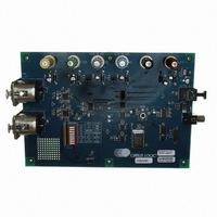
BOARD EVAL FOR CS5381 192KHZ ADC
Manufacturer
Cirrus Logic Inc
Specifications of CDB5381
Number Of Adc's
2
Number Of Bits
24
Sampling Rate (per Second)
192k
Data Interface
Serial
Inputs Per Adc
1 Differential
Input Range
6.1 Vpp
Power (typ) @ Conditions
360mW @ 5 V
Voltage Supply Source
Analog and Digital
Operating Temperature
-10°C ~ 70°C
Utilized Ic / Part
CS5381
Product
Audio Modules
Lead Free Status / RoHS Status
Contains lead / RoHS non-compliant
Lead Free Status / RoHS Status
Lead free / RoHS Compliant, Contains lead / RoHS non-compliant
Other names
598-1008


2
TABLE OF CONTENTS
1. PIN DESCRIPTIONS ............................................................................................................................... 4
2. CHARACTERISTICS AND SPECIFICATIONS....................................................................................... 5
SPECIFIED OPERATING CONDITIONS .................................................................................................... 5
ABSOLUTE MAXIMUM RATINGS............................................................................................................... 5
ANALOG CHARACTERISTICS (CS5381-KSZ/-KZZ).................................................................................. 6
DIGITAL FILTER CHARACTERISTICS....................................................................................................... 7
SWITCHING CHARACTERISTICS - SERIAL AUDIO PORT .................................................................... 10
DC ELECTRICAL CHARACTERISTICS.................................................................................................... 13
DIGITAL CHARACTERISTICS .................................................................................................................. 13
THERMAL CHARACTERISTICS .............................................................................................................. 13
TYPICAL CONNECTION DIAGRAM ......................................................................................................... 14
3. APPLICATIONS .................................................................................................................................... 15
4. PACKAGE DIMENSIONS ..................................................................................................................... 20
5. ORDERING INFORMATION ................................................................................................................. 22
7. REVISION HISTORY ............................................................................................................................. 24
3.1 Operational Mode/Sample Rate Range Select.............................................................................. 15
3.2 System Clocking ............................................................................................................................ 15
3.3 Power-Up Sequence ..................................................................................................................... 16
3.4 Analog Connections ...................................................................................................................... 16
3.5 High-Pass Filter and DC Offset Calibration .................................................................................. 17
3.6 Overflow Detection ........................................................................................................................ 18
3.7 Grounding and Power Supply Decoupling..................................................................................... 18
3.8 Synchronization of Multiple Devices .............................................................................................. 18
3.9 Capacitor Size on the Reference Pin (FILT+)................................................................................ 19
3.2.1 Master Mode ........................................................................................................................ 15
3.2.2 Slave Mode .......................................................................................................................... 16
3.6.1 OVFL Configuration ............................................................................................................. 18
3.6.2 OVFL Output Timing ............................................................................................................ 18
CS5381
DS563F2
Related parts for CDB5381
Image
Part Number
Description
Manufacturer
Datasheet
Request
R

Part Number:
Description:
Development Kit
Manufacturer:
Cirrus Logic Inc
Datasheet:
Part Number:
Description:
Development Kit
Manufacturer:
Cirrus Logic Inc
Datasheet:


Part Number:
Description:
High-efficiency PFC + Fluorescent Lamp Driver Reference Design
Manufacturer:
Cirrus Logic Inc
Datasheet:
Part Number:
Description:
Development Kit
Manufacturer:
Cirrus Logic Inc
Datasheet:
Part Number:
Description:
Development Kit
Manufacturer:
Cirrus Logic Inc
Datasheet:

Part Number:
Description:
Development Kit
Manufacturer:
Cirrus Logic Inc
Datasheet:
Part Number:
Description:
Development Kit
Manufacturer:
Cirrus Logic Inc
Datasheet:
Part Number:
Description:
Development Kit
Manufacturer:
Cirrus Logic Inc
Datasheet:
Part Number:
Description:
Development Kit
Manufacturer:
Cirrus Logic Inc
Datasheet:

Part Number:
Description:
EVALUATION BOARD FOR CS8427
Manufacturer:
Cirrus Logic Inc
Datasheet:

Part Number:
Description:
BOARD EVAL FOR CS8416 RCVR
Manufacturer:
Cirrus Logic Inc
Datasheet:

Part Number:
Description:
EVALUATION BOARD FOR CS8420
Manufacturer:
Cirrus Logic Inc
Datasheet:

Part Number:
Description:
KIT DEVELOPMENT EP9315 ARM9
Manufacturer:
Cirrus Logic Inc
Datasheet:

Part Number:
Description:
KIT DEVELOPMENT EP9302 ARM9
Manufacturer:
Cirrus Logic Inc
Datasheet: