STEVAL-ISA050V1 STMicroelectronics, STEVAL-ISA050V1 Datasheet - Page 30
STEVAL-ISA050V1
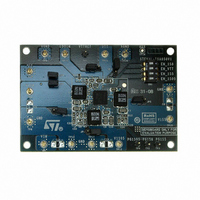
Manufacturer Part Number
STEVAL-ISA050V1
Description
KIT EVAL PM6641 CHIPSET/DDR2/3
Manufacturer
STMicroelectronics
Type
DC/DC Switching Converters, Regulators & Controllersr
Specifications of STEVAL-ISA050V1
Main Purpose
Special Purpose DC/DC, DDR Memory Supply
Outputs And Type
4, Non-Isolated
Power - Output
14.7W
Voltage - Output
1.05V, 1.5V, 1.8V, 0.9V
Current - Output
4A, 2.8A, 2.5A, 2A
Voltage - Input
2.7 ~ 5.5V
Regulator Topology
Buck
Frequency - Switching
750kHz
Board Type
Fully Populated
Utilized Ic / Part
PM6641
Input Voltage
2.7 V to 5.5 V
Product
Power Management Modules
Silicon Manufacturer
ST Micro
Silicon Core Number
PM6641
Kit Application Type
Power Management - Voltage Regulator
Application Sub Type
Monolithic Voltage Regulator
Kit Contents
Board
Lead Free Status / RoHS Status
Lead free / RoHS Compliant
For Use With/related Products
PM6641
Other names
497-8425
Available stocks
Company
Part Number
Manufacturer
Quantity
Price
Company:

Part Number:
STEVAL-ISA050V1
Manufacturer:
STMicroelectronics
Quantity:
1


Device description
7.9
30/47
Phase management
When all the three switching regulators high side MOSFETs are turned on simultaneously
the input root mean square (RMS) current could rise up to very high values, increasing the
system losses and inducing external components overheating. It’s possible to reduce the
input overall RMS current by inserting one ceramic capacitor as close as possible to each
switching regulator power supply input, reducing the impulsive input current path. However
this synchronous mode of operation is jitter-free and noise immune.
Another possible way to reduce the input RMS current is based on the phase shifting
technique, which decreases the total input current by delaying the regulators turn on pulse.
With three regulators turned on, the 120d e.g. phase shifting allows to reduce the overall
input current up to 1.73 times as depicted in the following configuration, in which three
independent regulators with Vout/Vin lower than 0.333 and identical output current (I) are
managed with synchronous or 120 deg phase shifted turning on.
Figure 32. SW regulator phase management
Each regulator RMS input current is easily computed:
Equation 7
defining T
SW
the switching period, equal to
I
I
I
Synchronous
I
L
L1
L2
L3
I
1
CIN
L ,
2
L ,
3
Doc ID 13510 Rev 3
+
+
=
=
T
SW
1
T
∫
SW
I
L
2
1
1
L ,
2
f
L ,
SW
3
dt
and T
=
120deg delay
I
I
L1
CIN
T
ON
+
+
=
SW
1
I
the high side MOSFET on time.
I
L2
2
T
ON
I
L3
PM6641
Related parts for STEVAL-ISA050V1
Image
Part Number
Description
Manufacturer
Datasheet
Request
R

Part Number:
Description:
BOARD RGB CTR ST7,STP08C596MTR
Manufacturer:
STMicroelectronics
Datasheet:

Part Number:
Description:
Power Management IC Development Tools Full Speed USB to RS232 Bridge Demo
Manufacturer:
STMicroelectronics
Datasheet:
Part Number:
Description:
Power Management IC Development Tools 2.5W solar eval BRD USB SPV1040 LD39050
Manufacturer:
STMicroelectronics
Datasheet:

Part Number:
Description:
BOARD EVAL FOR MEMS SENSORS
Manufacturer:
STMicroelectronics
Datasheet:

Part Number:
Description:
KIT DEV STARTER ST10F276Z5
Manufacturer:
STMicroelectronics
Datasheet:

Part Number:
Description:
BOARD EVAL HDMI $ VIDEO SWITCH
Manufacturer:
STMicroelectronics
Datasheet:

Part Number:
Description:
BOARD DEMO ACCELEROMETER DIL24
Manufacturer:
STMicroelectronics
Datasheet:

Part Number:
Description:
BOARD STLM75/STDS75/ST72F651
Manufacturer:
STMicroelectronics
Datasheet:

Part Number:
Description:
EVAL BOARD 3AXIS MEMS ACCELLRMTR
Manufacturer:
STMicroelectronics
Datasheet:

Part Number:
Description:
BOARD EVAL 8BIT MICRO + TDE1708
Manufacturer:
STMicroelectronics
Datasheet:
Part Number:
Description:
STMicroelectronics [RIPPLE-CARRY BINARY COUNTER/DIVIDERS]
Manufacturer:
STMicroelectronics
Datasheet:
Part Number:
Description:
STMicroelectronics [LIQUID-CRYSTAL DISPLAY DRIVERS]
Manufacturer:
STMicroelectronics
Datasheet:
Part Number:
Description:
BOARD EVAL FOR MEMS SENSORS
Manufacturer:
STMicroelectronics
Datasheet: