NCP1014STBUCGEVB ON Semiconductor, NCP1014STBUCGEVB Datasheet - Page 10
NCP1014STBUCGEVB
Manufacturer Part Number
NCP1014STBUCGEVB
Description
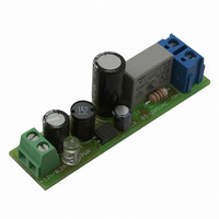
EVAL BOARD FOR NCP1014STBUCG
Manufacturer
ON Semiconductor
Datasheets
1.NCP1010ST100T3G.pdf
(24 pages)
2.NCP1014STBUCGEVB.pdf
(4 pages)
3.NCP1014STBUCGEVB.pdf
(1 pages)
Specifications of NCP1014STBUCGEVB
Design Resources
NCP1014STBUCGEVB BOM NCP1014STBUCGEVB Gerber Files NCP1014STBUCGEVB Schematic
Main Purpose
AC/DC, Non-Isolated
Outputs And Type
1, Non-Isolated
Voltage - Output
12V
Current - Output
0 ~ 3A, 0 ~ 3A, 5A
Voltage - Input
85 ~ 265VAC
Regulator Topology
Buck
Frequency - Switching
65kHz
Board Type
Fully Populated
Utilized Ic / Part
NCP1014
Lead Free Status / RoHS Status
Lead free / RoHS Compliant
Power - Output
-
Lead Free Status / Rohs Status
Lead free / RoHS Compliant
For Use With/related Products
NCP1014STBUCG
Other names
NCP1014STBUCGEVBOS


is expressed by:
the IC actually pulses is given by
Finally,
using the same formula topology:
From these three definitions, the burst duty- -cycle
can be computed:
equation with values extracted from the parameter section
gives a typical duty- -cycle of 13%, precluding any lethal
thermal runaway while in a fault condition.
DSS Internal Dissipation
drain pin. In Flyback- -based converters, this drain level can
easily go above 600 V peak and thus increase the stress on the
DSS startup source. However, the drain voltage evolves with
time and its period is small compared to that of the DSS. As
a result, the averaged dissipation, excluding capacitive losses,
can be derived by:
Figure 17 portrays a typical drain- -ground waveshape where
leakage effects have been removed.
dc =
The rising slope from the latch- -off level up to 8.5 V
The Dynamic Self- -Supplied pulls energy out from the
ICC1 ·
the
ICC1
ΔV2
ΔV2
Tstart =
latch- -off
+
P DSS = ICC1 · < Vds(t) > .
ΔV1
IC1
dc =
+
ΔV1 · C
ICC2
Tstart + Tsw + TLatch
ΔV3
IC1
Figure 16. NCP101X Facing a Fault Condition (Vin = 150 Vdc)
time
Tstart
(eq. 3)
. The time during which
Tsw
can
TLatch =
.
Tsw
tsw =
Feeding
be
ΔV3 · C
ΔV2 · C
derived
ICC2
ICC1
(eq. 2)
(eq. 4)
http://onsemi.com
the
TLatch
.
.
.
.
10
derived by additive square area calculation:
toff can be expressed by:
can be evaluated by:
1 V Ripple
By looking at Figure 17, the average result can easily be
By developing Equation 5, we obtain:
Vds(t)
Figure 17. A typical drain- -ground waveshape
where leakage effects are not accounted for.
Latch--off
< Vds(t) >= Vin − Vin · ton
Vin
Level
< Vds(t) >= Vin · (1 − d) + Vr · toff
ton
Vr
Tsw
ton = Ip ·
toff
toff = Ip ·
dt
Vin
Lp
Tsw
(eq. 8)
Lp
Vr
+ Vr · toff
(eq. 7)
.
Tsw
Tsw
where ton
(eq. 5)
(eq. 6)
t
Related parts for NCP1014STBUCGEVB
Image
Part Number
Description
Manufacturer
Datasheet
Request
R

Part Number:
Description:
ON Semiconductor [VOLTAGE REGULATOR]
Manufacturer:
ON Semiconductor
Datasheet:
Part Number:
Description:
357-036-542-201 CARDEDGE 36POS DL .156 BLK LOPRO
Manufacturer:
ON Semiconductor
Datasheet:
Part Number:
Description:
357-036-542-201 CARDEDGE 36POS DL .156 BLK LOPRO
Manufacturer:
ON Semiconductor
Datasheet:
Part Number:
Description:
357-036-542-201 CARDEDGE 36POS DL .156 BLK LOPRO
Manufacturer:
ON Semiconductor
Datasheet:
Part Number:
Description:
357-036-542-201 CARDEDGE 36POS DL .156 BLK LOPRO
Manufacturer:
ON Semiconductor
Datasheet:
Part Number:
Description:
357-036-542-201 CARDEDGE 36POS DL .156 BLK LOPRO
Manufacturer:
ON Semiconductor
Datasheet:
Part Number:
Description:
357-036-542-201 CARDEDGE 36POS DL .156 BLK LOPRO
Manufacturer:
ON Semiconductor
Datasheet:
Part Number:
Description:
357-036-542-201 CARDEDGE 36POS DL .156 BLK LOPRO
Manufacturer:
ON Semiconductor
Datasheet:
Part Number:
Description:
357-036-542-201 CARDEDGE 36POS DL .156 BLK LOPRO
Manufacturer:
ON Semiconductor
Datasheet:
Part Number:
Description:
357-036-542-201 CARDEDGE 36POS DL .156 BLK LOPRO
Manufacturer:
ON Semiconductor
Datasheet:
Part Number:
Description:
357-036-542-201 CARDEDGE 36POS DL .156 BLK LOPRO
Manufacturer:
ON Semiconductor
Datasheet:
Part Number:
Description:
Manufacturer:
ON Semiconductor
Datasheet:
Part Number:
Description:
Manufacturer:
ON Semiconductor
Datasheet:
Part Number:
Description:
Manufacturer:
ON Semiconductor
Datasheet: