NCP1014STBUCGEVB ON Semiconductor, NCP1014STBUCGEVB Datasheet - Page 5
NCP1014STBUCGEVB
Manufacturer Part Number
NCP1014STBUCGEVB
Description
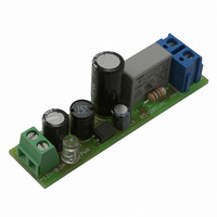
EVAL BOARD FOR NCP1014STBUCG
Manufacturer
ON Semiconductor
Datasheets
1.NCP1010ST100T3G.pdf
(24 pages)
2.NCP1014STBUCGEVB.pdf
(4 pages)
3.NCP1014STBUCGEVB.pdf
(1 pages)
Specifications of NCP1014STBUCGEVB
Design Resources
NCP1014STBUCGEVB BOM NCP1014STBUCGEVB Gerber Files NCP1014STBUCGEVB Schematic
Main Purpose
AC/DC, Non-Isolated
Outputs And Type
1, Non-Isolated
Voltage - Output
12V
Current - Output
0 ~ 3A, 0 ~ 3A, 5A
Voltage - Input
85 ~ 265VAC
Regulator Topology
Buck
Frequency - Switching
65kHz
Board Type
Fully Populated
Utilized Ic / Part
NCP1014
Lead Free Status / RoHS Status
Lead free / RoHS Compliant
Power - Output
-
Lead Free Status / Rohs Status
Lead free / RoHS Compliant
For Use With/related Products
NCP1014STBUCG
Other names
NCP1014STBUCGEVBOS


2. See characterization curves for temperature evolution.
3. Adjust di/dt to reach Ipeak in 3.2 msec.
ELECTRICAL CHARACTERISTICS
V
SUPPLY SECTION AND V
POWER SWITCH CIRCUIT
INTERNAL STARTUP CURRENT SOURCE
CURRENT COMPARATOR T
CC
V
V
Hysteresis between VCC
V
V
Internal IC Consumption, MOSFET Switching at 65 kHz (Note 2)
Internal IC Consumption, MOSFET Switching at 100 kHz (Note 2)
Internal IC Consumption, MOSFET Switching at 130 kHz (Note 2)
Internal IC Consumption, Latch--off Phase, V
Active Zener Voltage Positive Offset to VCC
Latch--off Current
Power Switch Circuit On--state Resistance
Power Switch Circuit and Startup Breakdown Voltage
Power Switch and Startup Breakdown Voltage Off--state Leakage Current
Switching Characteristics (RL = 50 Ω, Vds Set for Idrain = 0.7 x Ilim)
High--voltage Current Source, V
High--voltage Current Source, V
Maximum Internal Current Setpoint, NCP1010 (Note 3)
Maximum Internal Current Setpoint, NCP1011 (Note 3)
Maximum Internal Current Setpoint, NCP1012 (Note 3)
Maximum Internal Current Setpoint, NCP1013 (Note 3)
Maximum Internal Current Setpoint, NCP1014 (Note 3)
Default Internal Current Setpoint for Skip--Cycle Operation, Percentage of
Propagation Delay from Current Detection to Drain OFF State
Leading Edge Blanking Duration
CC
CC
CC
CC
NCP1012/13/14
NCP1010/11
NCP1012/13/14 (Id = 50 mA)
NCP1010/11 (Id = 50 mA)
(ID
NCP1012/13/14
NCP1010/11
Max Ip
= 8.0 V unless otherwise noted.)
T
T
T
T
T
T
T
Turn--on Time (90%--10%)
Turn--off Time (10%--90%)
Increasing Level at which the Current Source Turns--off
Decreasing Level at which the Current Source Turns--on
Decreasing Level at which the Latch--off Phase Ends
Decreasing Level at which the Internal Latch is Released
(off)
J
J
J
J
J
J
J
= 25C
= 125C
= 25C
= 125C
= --40C (Vds = 650 V)
= 25C (Vds = 700 V)
= 125C (Vds = 700 V)
= 120 mA, T
J
= 25C)
OFF
CC
J
MANAGEMENT
and VCC
= 25C (Note 2)
CC
CC
Rating
= 8.0 V
= 0
0C < T
--40C < T
0C < T
--40C < T
0C < T
--40C < T
0C < T
--40C < T
ON
(For typical values T
OFF
J
J
J
J
CC
< 125C
< 125C
< 125C
< 125C
J
J
J
J
= 6.0 V
< 125C
< 125C
< 125C
< 125C
http://onsemi.com
J
= 25C, for min/max values T
5
Pin
1
1
1
1
1
1
1
1
1
1
1
5
5
5
5
5
5
5
1
1
5
5
5
5
5
--
--
--
Ipeak (22)
Ipeak (22)
Ipeak (11)
Ipeak (11)
Ipeak (11)
VCC
VCC
VCC
Symbol
I
Vclamp
VCC
DS(OFF
BVdss
R
ILatch
ICC1
ICC1
ICC1
ICC2
I
T
T
J
Lskip
IC1
IC2
DSon
ton
toff
DEL
LEB
--
= --40C to +125C, Max T
reset
OFF
latch
ON
)
Min
140
700
225
225
315
405
7.9
6.9
4.4
6.3
5.8
5.8
5.3
5.0
5.0
5.0
5.0
90
--
--
--
--
--
--
--
--
--
--
--
--
--
--
--
--
0.92
0.95
0.98
Typ
290
200
100
250
250
350
450
125
250
8.5
7.5
1.0
4.7
3.0
7.4
7.4
7.3
7.3
8.0
8.0
8.0
8.0
19
22
38
70
50
30
20
10
10
25
11
--
J
= 150C,
Max
1.15
10.3
11.5
300
120
275
275
385
495
110
9.1
8.1
5.1
1.1
1.2
9.2
9.2
9.0
9.0
16
24
35
50
10
11
--
--
--
--
--
--
--
--
--
--
--
--
Unit
mA
mA
mA
mV
mA
mA
mA
mA
mA
mA
mA
mA
mA
mA
ns
ns
ns
%
V
V
V
V
V
Ω
V
Related parts for NCP1014STBUCGEVB
Image
Part Number
Description
Manufacturer
Datasheet
Request
R

Part Number:
Description:
ON Semiconductor [VOLTAGE REGULATOR]
Manufacturer:
ON Semiconductor
Datasheet:
Part Number:
Description:
357-036-542-201 CARDEDGE 36POS DL .156 BLK LOPRO
Manufacturer:
ON Semiconductor
Datasheet:
Part Number:
Description:
357-036-542-201 CARDEDGE 36POS DL .156 BLK LOPRO
Manufacturer:
ON Semiconductor
Datasheet:
Part Number:
Description:
357-036-542-201 CARDEDGE 36POS DL .156 BLK LOPRO
Manufacturer:
ON Semiconductor
Datasheet:
Part Number:
Description:
357-036-542-201 CARDEDGE 36POS DL .156 BLK LOPRO
Manufacturer:
ON Semiconductor
Datasheet:
Part Number:
Description:
357-036-542-201 CARDEDGE 36POS DL .156 BLK LOPRO
Manufacturer:
ON Semiconductor
Datasheet:
Part Number:
Description:
357-036-542-201 CARDEDGE 36POS DL .156 BLK LOPRO
Manufacturer:
ON Semiconductor
Datasheet:
Part Number:
Description:
357-036-542-201 CARDEDGE 36POS DL .156 BLK LOPRO
Manufacturer:
ON Semiconductor
Datasheet:
Part Number:
Description:
357-036-542-201 CARDEDGE 36POS DL .156 BLK LOPRO
Manufacturer:
ON Semiconductor
Datasheet:
Part Number:
Description:
357-036-542-201 CARDEDGE 36POS DL .156 BLK LOPRO
Manufacturer:
ON Semiconductor
Datasheet:
Part Number:
Description:
357-036-542-201 CARDEDGE 36POS DL .156 BLK LOPRO
Manufacturer:
ON Semiconductor
Datasheet:
Part Number:
Description:
Manufacturer:
ON Semiconductor
Datasheet:
Part Number:
Description:
Manufacturer:
ON Semiconductor
Datasheet:
Part Number:
Description:
Manufacturer:
ON Semiconductor
Datasheet: