AD9755-EB Analog Devices Inc, AD9755-EB Datasheet - Page 6
AD9755-EB
Manufacturer Part Number
AD9755-EB
Description
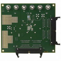
BOARD EVAL FOR AD9755
Manufacturer
Analog Devices Inc
Series
TxDAC+®r
Datasheet
1.AD9755ASTZ.pdf
(28 pages)
Specifications of AD9755-EB
Rohs Status
RoHS non-compliant
Number Of Dac's
1
Number Of Bits
14
Outputs And Type
1, Differential
Sampling Rate (per Second)
300M
Data Interface
Parallel
Settling Time
11ns
Dac Type
Current
Voltage Supply Source
Analog and Digital
Operating Temperature
-40°C ~ 85°C
Utilized Ic / Part
AD9755


AD9755
Pin No.
1
2
3
4, 22
5, 21
6
7–20
23–36
37, 38
39
40
41
42
43
44
45
46
47
48
Mnemonic
RESET
CLK+
CLK–
DCOM
DVDD
PLLLOCK
P1B13–P1B0
P2B13–P2B0
DIV0, DIV1
REFIO
FSADJ
AVDD
I
I
ACOM
CLKCOM
LPF
PLLVDD
CLKVDD
OUTB
OUTA
MSB–P1B13
PLLLOCK
RESET
DCOM
P1B12
P1B11
P1B10
DVDD
CLK+
CLK–
P1B9
P1B8
Description
Internal Clock Divider Reset
Differential Clock Input
Differential Clock Input
Digital Common
Digital Supply Voltage
Phase-Locked Loop Lock Indicator Output
Data Bits P1B13 to P1B0, Port 1
Data Bits P2B13 to P2B0, Port 2
Control Inputs for PLL and Input Port Selector Mode; see Tables I and II for details.
Reference Input/Output
Full-Scale Current Output Adjust
Analog Supply Voltage
Differential DAC Current Output
Differential DAC Current Output
Analog Common
Clock and Phase-Locked Loop Common
Phase-Locked Loop Filter
Phase-Locked Loop Supply Voltage
Clock Supply Voltage
PIN FUNCTION DESCRIPTIONS
10
11
12
1
2
3
4
5
6
7
8
9
48 47 46 45 44
13 14 15 16 17 18 19 20 21 22 23 24
PIN CONFIGURATION
PIN 1
IDENTIFIER
(Not to Scale)
AD9755
TOP VIEW
43 42 41 40
–6–
39 38 37
36
35
34
33
32
31
30
29
28
27
26
25
P2B0–LSB
P2B1
P2B2
P2B3
P2B4
P2B5
P2B6
P2B7
P2B8
P2B9
P2B10
P2B11
REV. B
Related parts for AD9755-EB
Image
Part Number
Description
Manufacturer
Datasheet
Request
R

Part Number:
Description:
±1.7g Dual-Axis IMEMS Accelerometer Evaluation Board
Manufacturer:
Analog Devices Inc
Datasheet:

Part Number:
Description:
Inertial Sensor Evaluation System
Manufacturer:
Analog Devices Inc
Datasheet:
Part Number:
Description:
Manufacturer:
Analog Devices Inc
Datasheet:
Part Number:
Description:
Manufacturer:
Analog Devices Inc
Datasheet:
Part Number:
Description:
Manufacturer:
Analog Devices Inc
Datasheet:
Part Number:
Description:
Manufacturer:
Analog Devices Inc
Datasheet:
Part Number:
Description:
Manufacturer:
Analog Devices Inc
Datasheet:
Part Number:
Description:
Manufacturer:
Analog Devices Inc
Datasheet:
Part Number:
Description:
Manufacturer:
Analog Devices Inc
Datasheet:
Part Number:
Description:
Manufacturer:
Analog Devices Inc
Datasheet:
Part Number:
Description:
Manufacturer:
Analog Devices Inc
Datasheet:
Part Number:
Description:
Manufacturer:
Analog Devices Inc
Datasheet:
Part Number:
Description:
Manufacturer:
Analog Devices Inc
Datasheet: