NCP3065SOBSTGEVB ON Semiconductor, NCP3065SOBSTGEVB Datasheet - Page 3
NCP3065SOBSTGEVB
Manufacturer Part Number
NCP3065SOBSTGEVB
Description
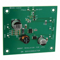
EVAL BOARD FOR NCP3065SOBSTG
Manufacturer
ON Semiconductor
Datasheets
1.NCP3065DR2G.pdf
(18 pages)
2.NCP3065SOBSTGEVB.pdf
(1 pages)
3.NCP3065SOBSTGEVB.pdf
(18 pages)
Specifications of NCP3065SOBSTGEVB
Design Resources
NCP3065 Boost Eval Board BOM NCP3065SOBSTGEVB Gerber Files NCP3065 Boost Eval Board Schematic
Current - Output / Channel
350mA
Outputs And Type
1, Non-Isolated
Voltage - Output
20 V
Voltage - Input
12V
Utilized Ic / Part
NCP3065
Core Chip
NCP3065
Topology
Buck-Boost
No. Of Outputs
1
Dimming Control Type
PWM
Development Tool Type
Hardware - Eval/Demo Board
Leaded Process Compatible
Yes
Mcu Supported Families
NCP3065
Rohs Compliant
Yes
Lead Free Status / RoHS Status
Lead free / RoHS Compliant
Features
-
Lead Free Status / Rohs Status
Lead free / RoHS Compliant
For Use With/related Products
NCP3065SOBSTG
Other names
NCP3065SOBSTGEVBOS


Stresses exceeding Maximum Ratings may damage the device. Maximum Ratings are stress ratings only. Functional operation above the
Recommended Operating Conditions is not implied. Extended exposure to stresses above the Recommended Operating Conditions may affect
device reliability.
1. This device series contains ESD protection and exceeds the following tests:
2. This device contains latch−up protection and exceeds 100 mA per JEDEC Standard JESD78.
3. The relation between junction temperature, ambient temperature and Total Power dissipated in IC is T
4. The pins which are not defined may not be loaded by external signals
MAXIMUM RATINGS
Power Dissipation and Thermal Characteristics
V
Comparator Inverting Input (Pin 5)
Darlington Switch Collector (Pin 1)
Darlington Switch Emitter (Pin 2) (Transistor OFF)
Darlington Switch Collector to Emitter (Pins 1−2)
Darlington Switch Current
I
Timing Capacitor (Pin 3)
PDIP−8
SOIC−8
DFN−8
Storage Temperature Range
Maximum Junction Temperature
Operating Junction Temperature Range (Note 3)
pk
CC
Thermal Resistance Junction−to−Air
Thermal Resistance Junction−to−Air
Thermal Resistance Junction−to−Air
Thermal Resistance Junction−to−Case
NCP3065, NCV3065
Sense (Pin 7)
Pin 1−8: Human Body Model 2000 V per AEC Q100−002; 003 or JESD22/A114; A115
Machine Model Method 200 V
(Pin 6)
(measured vs. pin 4, unless otherwise noted)
Rating
http://onsemi.com
3
Symbol
T
V
V
V
V
T
R
R
R
R
J(MAX)
V
V
V
SWCE
I
TCAP
SWC
SWE
SW
STG
T
IPK
qJA
qJA
qJA
qJC
CC
CII
J
−0.2 to V
−0.2 to +V
−0.6 to +V
−0.2 to +1.4
−65 to +150
−40 to +125
0 to +40
0 to +40
0 to +40
Value
+150
J
100
180
1.5
78
14
= T
CC
A
+ 0.2
CC
CC
+ R
q •
P
D
°C/W
°C/W
°C/W
Unit
°C
°C
°C
V
V
V
V
V
A
V
V
Related parts for NCP3065SOBSTGEVB
Image
Part Number
Description
Manufacturer
Datasheet
Request
R

Part Number:
Description:
Up to 1.5 A Constant Current Switching Regulator for LEDs
Manufacturer:
ON Semiconductor
Datasheet:

Part Number:
Description:
EVAL BOARD FOR NCP3065SOBCKG
Manufacturer:
ON Semiconductor
Datasheet:

Part Number:
Description:
EVAL BOARD FOR NCP30653ABCKG
Manufacturer:
ON Semiconductor
Datasheet:
Part Number:
Description:
ON Semiconductor [VOLTAGE REGULATOR]
Manufacturer:
ON Semiconductor
Datasheet:
Part Number:
Description:
357-036-542-201 CARDEDGE 36POS DL .156 BLK LOPRO
Manufacturer:
ON Semiconductor
Datasheet:
Part Number:
Description:
357-036-542-201 CARDEDGE 36POS DL .156 BLK LOPRO
Manufacturer:
ON Semiconductor
Datasheet:
Part Number:
Description:
357-036-542-201 CARDEDGE 36POS DL .156 BLK LOPRO
Manufacturer:
ON Semiconductor
Datasheet:
Part Number:
Description:
357-036-542-201 CARDEDGE 36POS DL .156 BLK LOPRO
Manufacturer:
ON Semiconductor
Datasheet:
Part Number:
Description:
357-036-542-201 CARDEDGE 36POS DL .156 BLK LOPRO
Manufacturer:
ON Semiconductor
Datasheet:
Part Number:
Description:
357-036-542-201 CARDEDGE 36POS DL .156 BLK LOPRO
Manufacturer:
ON Semiconductor
Datasheet:
Part Number:
Description:
357-036-542-201 CARDEDGE 36POS DL .156 BLK LOPRO
Manufacturer:
ON Semiconductor
Datasheet:
Part Number:
Description:
357-036-542-201 CARDEDGE 36POS DL .156 BLK LOPRO
Manufacturer:
ON Semiconductor
Datasheet:
Part Number:
Description:
357-036-542-201 CARDEDGE 36POS DL .156 BLK LOPRO
Manufacturer:
ON Semiconductor
Datasheet:
Part Number:
Description:
357-036-542-201 CARDEDGE 36POS DL .156 BLK LOPRO
Manufacturer:
ON Semiconductor
Datasheet: