NCP3065SOBSTGEVB ON Semiconductor, NCP3065SOBSTGEVB Datasheet - Page 4
NCP3065SOBSTGEVB
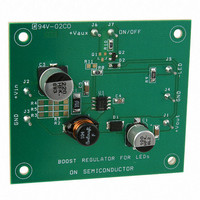
Manufacturer Part Number
NCP3065SOBSTGEVB
Description
EVAL BOARD FOR NCP3065SOBSTG
Manufacturer
ON Semiconductor
Datasheets
1.NCP3065DR2G.pdf
(18 pages)
2.NCP3065SOBSTGEVB.pdf
(1 pages)
3.NCP3065SOBSTGEVB.pdf
(18 pages)
Specifications of NCP3065SOBSTGEVB
Design Resources
NCP3065 Boost Eval Board BOM NCP3065SOBSTGEVB Gerber Files NCP3065 Boost Eval Board Schematic
Current - Output / Channel
350mA
Outputs And Type
1, Non-Isolated
Voltage - Output
20 V
Voltage - Input
12V
Utilized Ic / Part
NCP3065
Core Chip
NCP3065
Topology
Buck-Boost
No. Of Outputs
1
Dimming Control Type
PWM
Development Tool Type
Hardware - Eval/Demo Board
Leaded Process Compatible
Yes
Mcu Supported Families
NCP3065
Rohs Compliant
Yes
Lead Free Status / RoHS Status
Lead free / RoHS Compliant
Features
-
Lead Free Status / Rohs Status
Lead free / RoHS Compliant
For Use With/related Products
NCP3065SOBSTG
Other names
NCP3065SOBSTGEVBOS


5. Low duty cycle pulse techniques are used during test to maintain junction temperature as close to ambient temperature as possible.
6. The
7. NCV prefix is for automotive and other applications requiring site and change control.
ELECTRICAL CHARACTERISTICS
Emitter Voltage Drop
OSCILLATOR
OUTPUT SWITCH (Note 5)
Darlington Switch Collector to
Collector Off−State Current
COMPARATOR
TOTAL DEVICE
Frequency
Discharge to Charge Current Ratio
Capacitor Discharging Current
Capacitor Charging Current
Current Limit Sense Voltage
Threshold Voltage
Threshold Voltage Line Regulation
Input Bias Current
Supply Current
Thermal Shutdown Threshold
Hysteresis
on comparator response time and di/dt current slope. See the Operating Description section for details.
V
IPK(Sense)
Characteristic
Current Limit Sense Voltage is specified at static conditions. In dynamic operation the sensed current turn−off value depends
(V
CC
VPin 5 > V
(VPin 5 = 0 V, CT = 2.2 nF,
CT = 2.2 nF, Pin 7 = V
(Pin 7 to V
(Pin 7 to V
(Pin 7 to V
= 5.0 V, T
T
(V
(V
remaining pins open)
(T
T
J
J
CC
CC
= −40°C to +125°C
J
T
= 25°C) (Note 5)
= 25°C) (Note 6)
(I
(V
J
Conditions
T
SW
= 3.0 V to 40 V)
(V
T
= 0 to +85°C
= 5.0 V to 40 V,
CE
J
J
in
th
J
= 25°C)
CC
CC
CC
= 25°C
= 1.0 A,
, Pin 2 = GND,
= −40°C to +125°C, unless otherwise specified)
http://onsemi.com
= 40 V)
= V
, T
, T
, T
th
J
J
J
)
= 25°C)
= 25°C)
= 25°C)
4
CC
,
V
V
SWCE(DROP)
I
REG
Symbol
I
IPK(Sense)
DISCHG
I
DISCHG
C(OFF)
I
I
I
f
V
V
OSC
CHG
CHG
CII in
I
CC
TH
TH
LiNE
/
−1000
−6.0
Min
110
165
−10
5.5
1650
−100
0.01
Typ
150
275
185
235
160
6.0
1.0
±5
10
1000
Max
190
235
100
+10
6.5
1.3
6.0
7.0
Unit
kHz
mV
mV
mV
mA
mA
mA
mA
nA
°C
°C
%
%
V
−
Related parts for NCP3065SOBSTGEVB
Image
Part Number
Description
Manufacturer
Datasheet
Request
R

Part Number:
Description:
Up to 1.5 A Constant Current Switching Regulator for LEDs
Manufacturer:
ON Semiconductor
Datasheet:

Part Number:
Description:
EVAL BOARD FOR NCP3065SOBCKG
Manufacturer:
ON Semiconductor
Datasheet:

Part Number:
Description:
EVAL BOARD FOR NCP30653ABCKG
Manufacturer:
ON Semiconductor
Datasheet:
Part Number:
Description:
ON Semiconductor [VOLTAGE REGULATOR]
Manufacturer:
ON Semiconductor
Datasheet:
Part Number:
Description:
357-036-542-201 CARDEDGE 36POS DL .156 BLK LOPRO
Manufacturer:
ON Semiconductor
Datasheet:
Part Number:
Description:
357-036-542-201 CARDEDGE 36POS DL .156 BLK LOPRO
Manufacturer:
ON Semiconductor
Datasheet:
Part Number:
Description:
357-036-542-201 CARDEDGE 36POS DL .156 BLK LOPRO
Manufacturer:
ON Semiconductor
Datasheet:
Part Number:
Description:
357-036-542-201 CARDEDGE 36POS DL .156 BLK LOPRO
Manufacturer:
ON Semiconductor
Datasheet:
Part Number:
Description:
357-036-542-201 CARDEDGE 36POS DL .156 BLK LOPRO
Manufacturer:
ON Semiconductor
Datasheet:
Part Number:
Description:
357-036-542-201 CARDEDGE 36POS DL .156 BLK LOPRO
Manufacturer:
ON Semiconductor
Datasheet:
Part Number:
Description:
357-036-542-201 CARDEDGE 36POS DL .156 BLK LOPRO
Manufacturer:
ON Semiconductor
Datasheet:
Part Number:
Description:
357-036-542-201 CARDEDGE 36POS DL .156 BLK LOPRO
Manufacturer:
ON Semiconductor
Datasheet:
Part Number:
Description:
357-036-542-201 CARDEDGE 36POS DL .156 BLK LOPRO
Manufacturer:
ON Semiconductor
Datasheet:
Part Number:
Description:
357-036-542-201 CARDEDGE 36POS DL .156 BLK LOPRO
Manufacturer:
ON Semiconductor
Datasheet: