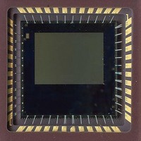
CYIL1SM0300-EVAL Cypress Semiconductor Corp, CYIL1SM0300-EVAL Datasheet
CYIL1SM0300-EVAL
Specifications of CYIL1SM0300-EVAL


Related parts for CYIL1SM0300-EVAL

CYIL1SM0300-EVAL Summary of contents
Page 1
... The sensor is available in a monochrome version or Bayer (RGB) patterned color filter array. This data sheet allows the user to develop a camera-system based on the described timing and interfacing. • 198 Champion Court • San Jose CYIL1SM0300AA , CA 95134-1709 • 408-943-2600 Revised October 15, 2009 [+] Feedback ...
Page 2
... Ordering Information Marketing Part Number CYIL1SM0300AA-QDC CYIL1SM0300AA-QWC CYIL1SE0300AA-QDC CYIL1SM0300AA-WWC CYIL1SM0300-EVAL CYIL1SE0300-EVAL Specifications General Specifications Parameter Specifications Pixel Architecture 6 transistor pixel Pixel Size 9.9 µm x 9.9 µm Resolution 640 x 480 Pixel Rate 80 MHz Shutter Type Pipelined snapshot shutter Frame Rate 250 fps ...
Page 3
... Photo-voltaic Response Curve 1.2 1 0.8 0.6 0.4 0.2 0 0.00E+00 1.00E+04 Document Number: 001-00371 Rev. *F Figure 2. Special Response of LUPA-300 600 700 Wavelength (nm) Figure 3. Photo-voltaic Response LUPA-300 2.00E+04 3.00E+04 4.00E+04 electrons CYIL1SM0300AA 800 900 1000 5.00E+04 6.00E+04 7.00E+04 Page [+] Feedback ...
Page 4
... Absolute Ratings are those values beyond which damage to the device may occur supply to digital circuit DDD DDA DDD Document Number: 001-00371 Rev. *F Specification/Description Parameter Value –0.5 to 3.5 –0.5 to 3.5 –0.5 to 3.5 +/– 50 350 to analog circuit) DDA CYIL1SM0300AA Unit ºC Page [+] Feedback ...
Page 5
... ADCs are multiplexed to one output bus operating at 80 MHz. Figure 4. Floor Plan of the Sensor On chip drivers Pixel array 640 x 480 Column amplifiers X-shift register PGA + ADC PGA + ADC PGA + ADC Mux 10 bit output CYIL1SM0300AA Typ Max Unit 2.5 V 2.5 V 2.5 V 3.3 3 ...
Page 6
... Comment 1200 clock periods for GRAN<1:0> 624 clock periods for GRAN<1:0> 336 clock periods for GRAN<1:0> 192 clock periods for GRAN<1:0> clock periods for GRAN<1:0> clock periods for GRAN<1:0> clock periods for GRAN<1:0> clock periods for GRAN<1:0> CYIL1SM0300AA Clarification Page [+] Feedback ...
Page 7
... Note that the FPN (fixed pattern noise) of the sensor causes a spread of about 100 mV on the dark level. To allow FPN correction during post processing of the image, this spread on the dark level needs to be covered by the input range of the ADC. CYIL1SM0300AA Comment Sub sampling Windowing Figure 6 ...
Page 8
... The red and blue histograms have a swing of 100 mV. This means the input range of the ADC is not completely used. By amplifying the signal with a factor 10 by the PGA, the full range of the ADC can be used. In this example, Vcal is set at 1.75V (the CYIL1SM0300AA Gain 1.32 1.56 1 ...
Page 9
... Note that no power supply filtering on chip is implemented and that noise on these power supplies can contribute immediately to the noise on the signal. The voltage supplies V V are especially important to be noise free. ADC CYIL1SM0300AA Table 8 and Table Table 8 summarizes the supplies related with all Description Power supply analog readout module ...
Page 10
... In slave mode: Input to control integration time. Active high Sequencer reset. Active low Readout clock (80 MHz), sine or square clock Enable of the SPI Clock of the SPI. (Max. 20 MHz) Data line of the SPI. Bidirectional pin CYIL1SM0300AA Related Module DC-Level‘ ADC 693 mV ADC Pixel array precharge ...
Page 11
... Essentially an active pixel array is read multiple times, and reset only once. The external system intelligence takes care of the interpretation of the data. Table 12 disadvantages of non destructive readout CYIL1SM0300AA Time axis [6] time summarizes the advantages ...
Page 12
... Position of reset TS pulse in number of lines Default <11:0>: 000000000000 FT_TIMER Position of frame transfer in number of lines Default <11:0>: 000111100001 VCAL DAC input for vcal Default <7:0>: 01001010 VBLACK DAC input for vblack Default <7:0>: 01101011 VOFFSET DAC input for voffset Default <7:0>: 01010101 CYIL1SM0300AA Description Page [+] Feedback ...
Page 13
... Dual slope is enabled (configured according to the RES2_TIMER register) 0: Dual slope is disabled (RES2_timer register is ignored) - default Res3_enable (1bit) This bit enables/disables the triple slope mode of the device. 1: triple slope is enabled (configured according to the RES3_TIMER register) 0: triple slope is disabled (RES3_timer register is ignored) - default CYIL1SM0300AA Description Page [+] Feedback ...
Page 14
... DS high = (Res2_timer-1) * (ROT + Nr. Pixels * clock period) Res3_timer <11:0> Document Number: 001-00371 Rev. *F CYIL1SM0300AA This register defines the position of the additional reset pulse to enable the triple slope capability. This is also defined as a number of lines - 1. The actual time on which the additional reset is given is calcu- lated with the following formula: TS high = (Res3_timer-1) * (ROT + Nr ...
Page 15
... Data Interface (SPI) The serial-3-wire interface (or Serial-to-Parallel Interface) uses a serial input to shift the data in the register buffer. When the complete data word is shifted into the register buffer the data word is loaded into the internal register where it is decoded. CYIL1SM0300AA Page [+] Feedback ...
Page 16
... The selection between master and slave mode is done by the MASTERMODE register of the SPI. The sequencer is clocked on the core clock; this is the same clock as the ADCs. The core clock is the input clock divided by 4. CYIL1SM0300AA b<3> b<2> b<1> b<0> ...
Page 17
... FT_TIMER <11:0>: The number of lines read out (minus 1) after which the Frame Transfer (FT) and the FOT starts. The length of the pulse is given by the formula: 4*(12*(GRAN<1:0>+1)+1) (in clock cycles). Figure 15. Integration Timing in Master Mode Res2_timer Res3_timer CYIL1SM0300AA L480 K160 FOT 1 FT_timer Res1_length ...
Page 18
... The integration time is set by the FT_TIMER register. The actual windowing achieved when the surrounding system discards the lines which are not desired for the selected window. CYIL1SM0300AA illustrates this. The internal pixel length of the ...
Page 19
... INT_TIME pins active low simultaneously. There is always a small delay between the applied external signals and the actual internally generated pulses. These delays are also shown in Figure 19. CYIL1SM0300AA Page [+] Feedback ...
Page 20
... LINE_VALIDs FRAME_VALID is low, must be discarded. Figure 21 illustrate this. Note The FRAME_VALID signal automically goes low after 480 LINE_VALID pulses in mastermode. Figure 20. LINE_VALID Timing. Valid Valid Valid Invalid CYIL1SM0300AA Simultanious min 12 clk periods FOT min 12 clk periods TS Integration Time are valid. LINE_VALIDs ...
Page 21
... LINE_VALID of the desired readout window. Readout Reset Integration 2. At time read_t after the last valid LINE_VALID of the desired window size, all other LINE_VALIDs should be ignored. 3. After the desired integration length all INT_TIME_x should simultaneous go low to start the FOT. CYIL1SM0300AA VALID INVALID FOT Page [+] Feedback ...
Page 22
... SPI upload INVALID RESET_N the internal clock is restarted. The SPI settings are not affected by RESET_N. If needed the SPI settings can be changed during a low level of RESET_N. Figure 24. Sequencer Reset Timing Min 50 ns INVALID CYIL1SM0300AA Dummy FOT SPI upload if required Normal operation Page [+] Feedback ...
Page 23
... Connect with 68 kΩ to VPIX and decouple with 100 nF to GND_DRIVERS Indicates when valid data is at the outputs. Active high Indicates when valid frame is readout In master mode: Output to indicate the triple slope integration time. In slave mode: Input to control the triple slope integration time CYIL1SM0300AA Page [+] Feedback ...
Page 24
... Sequencer reset, active low Readout clock (80 MHz), sine or square clock Power supply of the ADCs (2.5V) Ground supply of the ADCs Power supply of the output drivers (2.5V) Ground supply of the output drivers Databit<0> (LSB) Databit<1> Databit<2> Databit<3> Databit<4> Power supply of the ADCs (2.5V) CYIL1SM0300AA Page [+] Feedback ...
Page 25
... Package Drawing Document Number: 001-00371 Rev. *F Figure 25. Package Drawing CYIL1SM0300AA Page [+] Feedback ...
Page 26
... Package with Glass Die Specifications Pixel 0,0 Document Number: 001-00371 Rev ± 0.010m ± 0.13m m 8.6mm CYIL1SM0300AA ± ± 0.076m ± 0.076m ± 0.05m m Page [+] Feedback ...
Page 27
... Die in Package 31 Document Number: 001-00371 Rev. *F 7.1mm Optical center 48 1 CYIL1SM0300AA 19 7 Page [+] Feedback ...
Page 28
... Bonding Diagram Document Number: 001-00371 Rev. *F CYIL1SM0300AA Page [+] Feedback ...
Page 29
... Color Filter The LUPA-300 can also be processed with a Bayer RGB color pattern. Pixel (0,0) has a red filter Figure 27. Color Filter Arrangement on the Pixels Document Number: 001-00371 Rev. *F 600 700 Wavelength [nm ] CYIL1SM0300AA Figure 26 shows the transmission 800 900 Page [+] Feedback ...
Page 30
... It is important to note that pixel signals above the double slope reset level are not influ- enced by this double slope reset pulse (p1 and p2). If desired, additional reset pulses can be given at lower levels to achieve multiple slope. CYIL1SM0300AA Reset level 1 Reset level 2 Saturation level Page ...
Page 31
... Document History Page Document Title: CYIL1SM0300AA LUPA-300 CMOS Image Sensor Document Number: 001-00371 Submission Orig. of Rev. ECN. Date Change ** 386743 See ECN FPW *A 391272 See ECN FPW *B 422288 See ECN FPW *C 497126 See ECN QGS *D 645720 See ECN FPW *E 2766198 09/19/09 ...