CYIL1SM0300-EVAL Cypress Semiconductor Corp, CYIL1SM0300-EVAL Datasheet - Page 18
CYIL1SM0300-EVAL
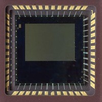
Manufacturer Part Number
CYIL1SM0300-EVAL
Description
BOARD EVAL IMAGE SENSOR LUPA-300
Manufacturer
Cypress Semiconductor Corp
Specifications of CYIL1SM0300-EVAL
Sensor Type
CMOS Imaging, Monochrome
Sensing Range
VGA
Interface
SPI
Sensitivity
250 fps
Voltage - Supply
2.5 V ~ 3.3 V
Embedded
No
Utilized Ic / Part
LUPA-300
Lead Free Status / RoHS Status
Contains lead / RoHS non-compliant
Lead Free Status / RoHS Status
Lead free / RoHS Compliant, Contains lead / RoHS non-compliant


The line counter starts with the value 1 immediately after the
rising edge of RESET_N and after the end of the FOT. This
means that the four integration timing registers must be
uploaded with the desired number of lines plus one.
In subsampling mode, the line counter increases with steps of
two. In this mode, the counter starts with the value ‘2’ immedi-
ately with the rising edge of RESET_N. This means that for
correct operation, the four integration timing registers can only
be uploaded with an even number of lines if subsampling is
enabled.
Readout Time Smaller Than or Equal to Integration Time
In this situation the RES_LENGTH register can be uploaded with
the smallest possible value, this is the value '2'. The frame rate
is determined by the integration time. The readout time is equal
to the integration time, the FT_TIMER register is uploaded with
a value equal to the window size to readout plus one. In case the
readout time is smaller than the integration time the FT_TIMER
register is uploaded with a value bigger than the window size.
Document Number: 001-00371 Rev. *F
INT_TIME1
INT_TIME2
INT_TIME3
SAMPLE
(internal )
RESET_N
Transfer
RESET
RESET
RESET
Frame
PIXEL
DS
TS
Figure 16. INT_TIME Timing
The length of the integration time, the DS integration time and
the TS integration time are indicated by 3 output pins:
INT_TIME_1, INT_TIME_2 and INT_TIME_3. These outputs are
high during the actual integration time. This is from the falling
edge of the corresponding reset pulse to the falling edge of the
internal pixel sample.
sample rises at the moment defined by FT_TIMER (see
Figure
4*(12*(GRAN<1:0>+1)+2).
Figure 17
the FRAME_VALID signal goes high to indicate the time needed
to read out the sensor.
When windowing in Y direction is desired in this mode (longer
integration time than read out time) the following parameters
should be set: The integration time is set by the FT_TIMER
register. The actual windowing in Y is achieved when the
surrounding system discards the lines which are not desired for
the selected window.
Total Integration Time
15)
shows this principle. While the sensor is being readout
DS Integration Time
and
Figure 16
the
TS Integration
Time
length
illustrates this. The internal pixel
CYIL1SM0300AA
of
the
Page 18 of 31
pulse
is
[+] Feedback
Related parts for CYIL1SM0300-EVAL
Image
Part Number
Description
Manufacturer
Datasheet
Request
R

Part Number:
Description:
Manufacturer:
Cypress Semiconductor Corp
Datasheet:
Part Number:
Description:
Manufacturer:
Cypress Semiconductor Corp
Datasheet:
Part Number:
Description:
Manufacturer:
Cypress Semiconductor Corp
Datasheet:
Part Number:
Description:
Manufacturer:
Cypress Semiconductor Corp
Datasheet:
Part Number:
Description:
Manufacturer:
Cypress Semiconductor Corp
Datasheet: