C8051F540DK Silicon Laboratories Inc, C8051F540DK Datasheet - Page 11
C8051F540DK
Manufacturer Part Number
C8051F540DK
Description
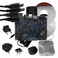
KIT DEVELOPMENT FOR C8051F540
Manufacturer
Silicon Laboratories Inc
Type
MCUr
Datasheet
1.C8051F540DK.pdf
(22 pages)
Specifications of C8051F540DK
Contents
Evaluation Board, Power Supply, USB Cables, Adapter and Documentation
Processor To Be Evaluated
C8051F54x
Processor Series
C8051F54x
Interface Type
USB
Operating Supply Voltage
5 V
Lead Free Status / RoHS Status
Lead free / RoHS Compliant
For Use With/related Products
C8051F54x
Lead Free Status / Rohs Status
Lead free / RoHS Compliant
Other names
336-1669


7.4. Switches and LEDs (J11, J16)
Two push-button switches are provided on the target board for each MCU. Switch RESET_A is connected to the
RST pin of the C8051F540. Switch RESET_B is connected to the RST pin of the C8051F542. Pressing RESET_A
puts the C8051F540 device into its hardware-reset state, and similarly for RESET_B and the C8051F542 MCU.
Switches P1.4_A and P1.4_B are connected to the MCU’s general purpose I/O (GPIO) pins through headers.
Pressing either one of these switches generates a logic low signal on the port pin. Remove the shorting block from
the header to disconnect these switches from the port pins. See Table 1 for the port pins and headers
corresponding to each switch.
Four LEDs are provided on the target board to serve as indicators. The red LED labeled PWR indicates presence
of power to the target board. The second red LED labeled COMM indicates if the CP2102 USB-to-UART bridge is
recognized by the PC. The green LED on Side A is labeled with port pin name and is connected to a C8051F580
GPIO pin through a header. Remove the shorting block from the header to disconnect the LED from the port pin.
Similarly, a second green LED on Side B is connected to the C8051F542 through another header. See Table 1 for
the port pins and headers corresponding to each LED.
7.5. Target Board Debug Interfaces (P2 and P3)
The debug connectors P2 (DEBUG_A) and P3 (DEBUG_B) provide access to the debug (C2) pins of the
C8051F540 and C8051F542. The debug connectors are used to connect the Serial Adapter or the USB Debug
Adapter to the target board for in-circuit debugging and Flash programming. Table 2 shows the DEBUG pin
definitions.
2, 3, 9
Pin #
10
1
4
5
6
7
8
Side A - C8051F540
USB Power (+5VDC from P2)
Red LED (COMM)
RST_A (Reset)
Not Connected
Not Connected
GND (Ground)
Red LED (PWR)
RST/C2CK_A
Description
P2.1_C2D_A
P1.4_A Switch
P1.4_B Switch
Description
P1.3_A LED
P1.3_B LED
Table 2. DEBUG Connector Pin Descriptions
RESET_A
RESET_B
P2.1
Table 1. Target Board I/O Descriptions
Rev. 0.1
Reset (Side A)
Reset (Side B)
COMM Active
P1.4 (Side A)
P1.4 (Side B)
P1.3 (Side A)
P1.3 (Side B)
Power
I/O
2, 3, 9
Pin #
10
1
4
5
6
7
8
Side B - C8051F542
Header(s)
J16[1–2]
J16[3–4]
J11[1–2]
J11[3–4]
RST_B (Reset)
Not Connected
Not Connected
Not Connected
none
none
none
GND (Ground)
none
RST/C2CK_B
Description
P2.1_C2D_B
C8051F540DK
P2.1_B
11
Related parts for C8051F540DK
Image
Part Number
Description
Manufacturer
Datasheet
Request
R

Part Number:
Description:
SMD/C°/SINGLE-ENDED OUTPUT SILICON OSCILLATOR
Manufacturer:
Silicon Laboratories Inc
Part Number:
Description:
Manufacturer:
Silicon Laboratories Inc
Datasheet:
Part Number:
Description:
N/A N/A/SI4010 AES KEYFOB DEMO WITH LCD RX
Manufacturer:
Silicon Laboratories Inc
Datasheet:
Part Number:
Description:
N/A N/A/SI4010 SIMPLIFIED KEY FOB DEMO WITH LED RX
Manufacturer:
Silicon Laboratories Inc
Datasheet:
Part Number:
Description:
N/A/-40 TO 85 OC/EZLINK MODULE; F930/4432 HIGH BAND (REV E/B1)
Manufacturer:
Silicon Laboratories Inc
Part Number:
Description:
EZLink Module; F930/4432 Low Band (rev e/B1)
Manufacturer:
Silicon Laboratories Inc
Part Number:
Description:
I°/4460 10 DBM RADIO TEST CARD 434 MHZ
Manufacturer:
Silicon Laboratories Inc
Part Number:
Description:
I°/4461 14 DBM RADIO TEST CARD 868 MHZ
Manufacturer:
Silicon Laboratories Inc
Part Number:
Description:
I°/4463 20 DBM RFSWITCH RADIO TEST CARD 460 MHZ
Manufacturer:
Silicon Laboratories Inc
Part Number:
Description:
I°/4463 20 DBM RADIO TEST CARD 868 MHZ
Manufacturer:
Silicon Laboratories Inc
Part Number:
Description:
I°/4463 27 DBM RADIO TEST CARD 868 MHZ
Manufacturer:
Silicon Laboratories Inc
Part Number:
Description:
I°/4463 SKYWORKS 30 DBM RADIO TEST CARD 915 MHZ
Manufacturer:
Silicon Laboratories Inc
Part Number:
Description:
N/A N/A/-40 TO 85 OC/4463 RFMD 30 DBM RADIO TEST CARD 915 MHZ
Manufacturer:
Silicon Laboratories Inc
Part Number:
Description:
I°/4463 20 DBM RADIO TEST CARD 169 MHZ
Manufacturer:
Silicon Laboratories Inc