C8051F540DK Silicon Laboratories Inc, C8051F540DK Datasheet - Page 14
C8051F540DK
Manufacturer Part Number
C8051F540DK
Description
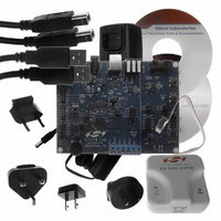
KIT DEVELOPMENT FOR C8051F540
Manufacturer
Silicon Laboratories Inc
Type
MCUr
Datasheet
1.C8051F540DK.pdf
(22 pages)
Specifications of C8051F540DK
Contents
Evaluation Board, Power Supply, USB Cables, Adapter and Documentation
Processor To Be Evaluated
C8051F54x
Processor Series
C8051F54x
Interface Type
USB
Operating Supply Voltage
5 V
Lead Free Status / RoHS Status
Lead free / RoHS Compliant
For Use With/related Products
C8051F54x
Lead Free Status / Rohs Status
Lead free / RoHS Compliant
Other names
336-1669


C8051F540DK
7.11. Power Supply I/O (Side A) (TB3)
All of the C8051F540 target device’s supply pins are connected to the TB3 terminal block. Refer to Table 8 for the
TB3 terminal block connections.
7.12. Alternate Power Supply Headers (J15, J18)
The C8051F540 Target Board includes two headers that allow for alternate power sources and power
measurement. Header J15 connects the VIO voltage supplied to the Side A MCU to other peripherals on the board,
such as the P1.4_SW push-button switch pull-up, and the R17 potentiometer source. To enable current
measurement, the shorting block on J15 can be removed so that the VIO_A node only powers the VIO pin on the
MCU. Another voltage source will need to be applied to the VIO_SRC node to power the other peripherals.
Header J18 connects the P4 power-adapter supply to the V_HIGH node, which is used as the power source for the
LIN transceivers (T1, T2). The shorting block on header J18 can be removed to force the LIN transceivers to use
the voltage supply externally supplied on the +LIN_V pin on the TB1 header.
7.13. C2 Pin Sharing
On the C8051F540 (Side A), the debug pins C2CK and C2D are shared with the pins RST and P2.1, respectively.
On the C8051F542 (Side B), the debug pins C2CK and C2D are shared with the pins RST and P2.1, respectively.
The target board includes the resistors necessary to enable pin sharing which allow the pin–shared pins (RST and
P3.0) to be used normally while simultaneously debugging the device. See Application Note “AN124: Pin Sharing
Techniques for the C2 Interface” at
14
Table 8. TB3 Terminal Block Pin Descriptions
www.silabs.com
Pin #
1
2
3
4
5
6
for more information regarding pin sharing.
Rev. 0.1
Description
VREGIN_A
GNDA_A
VDDA_A
VDD_A
VIO_A
GND
Related parts for C8051F540DK
Image
Part Number
Description
Manufacturer
Datasheet
Request
R

Part Number:
Description:
SMD/C°/SINGLE-ENDED OUTPUT SILICON OSCILLATOR
Manufacturer:
Silicon Laboratories Inc
Part Number:
Description:
Manufacturer:
Silicon Laboratories Inc
Datasheet:
Part Number:
Description:
N/A N/A/SI4010 AES KEYFOB DEMO WITH LCD RX
Manufacturer:
Silicon Laboratories Inc
Datasheet:
Part Number:
Description:
N/A N/A/SI4010 SIMPLIFIED KEY FOB DEMO WITH LED RX
Manufacturer:
Silicon Laboratories Inc
Datasheet:
Part Number:
Description:
N/A/-40 TO 85 OC/EZLINK MODULE; F930/4432 HIGH BAND (REV E/B1)
Manufacturer:
Silicon Laboratories Inc
Part Number:
Description:
EZLink Module; F930/4432 Low Band (rev e/B1)
Manufacturer:
Silicon Laboratories Inc
Part Number:
Description:
I°/4460 10 DBM RADIO TEST CARD 434 MHZ
Manufacturer:
Silicon Laboratories Inc
Part Number:
Description:
I°/4461 14 DBM RADIO TEST CARD 868 MHZ
Manufacturer:
Silicon Laboratories Inc
Part Number:
Description:
I°/4463 20 DBM RFSWITCH RADIO TEST CARD 460 MHZ
Manufacturer:
Silicon Laboratories Inc
Part Number:
Description:
I°/4463 20 DBM RADIO TEST CARD 868 MHZ
Manufacturer:
Silicon Laboratories Inc
Part Number:
Description:
I°/4463 27 DBM RADIO TEST CARD 868 MHZ
Manufacturer:
Silicon Laboratories Inc
Part Number:
Description:
I°/4463 SKYWORKS 30 DBM RADIO TEST CARD 915 MHZ
Manufacturer:
Silicon Laboratories Inc
Part Number:
Description:
N/A N/A/-40 TO 85 OC/4463 RFMD 30 DBM RADIO TEST CARD 915 MHZ
Manufacturer:
Silicon Laboratories Inc
Part Number:
Description:
I°/4463 20 DBM RADIO TEST CARD 169 MHZ
Manufacturer:
Silicon Laboratories Inc