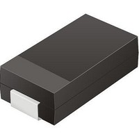
TV04A171JB-G Comchip Technology, TV04A171JB-G Datasheet - Page 16
TV04A171JB-G
Manufacturer Part Number
TV04A171JB-G
Description
TVS 400W 170V BIDIRECT SMA
Manufacturer
Comchip Technology
Specifications of TV04A171JB-G
Voltage - Reverse Standoff (typ)
170V
Voltage - Breakdown
189V
Power (watts)
400W
Polarization
Bidirectional
Mounting Type
Surface Mount
Package / Case
DO-214AC, SMA
Channels
1 Channel
Clamping Voltage
275 V
Operating Voltage
3.5 V
Breakdown Voltage
189 V
Peak Surge Current
40 A
Peak Pulse Power Dissipation
400 W
Lead Free Status / RoHS Status
Lead free / RoHS Compliant


7.6
7.7
16
Automatic Sleep Mode
RESET#: Hardware Reset Pin
The automatic sleep mode minimizes Flash device energy consumption. The device automatically enables
this mode when addresses remain stable for t
CE#, WE#, and OE# control signals. Standard address access timings provide new data when addresses are
changed. While in sleep mode, output data is latched and always available to the system. I
Characteristics on page 40
The RESET# pin provides a hardware method of resetting the device to reading array data. When the system
drives the RESET# pin to V
progress, tristates all data output pins, and ignores all read/write attempts for the duration of the RESET#
pulse. The device also resets the internal state machine to reading array data. The operation that was
interrupted should be reinitiated once the device is ready to accept another command sequence, to ensure
data integrity.
Current is reduced for the duration of the RESET# pulse. When RESET# is held at V
draws CMOS standby current (I
current will be greater.
The RESET# pin may be tied to the system reset circuitry. A system reset would thus also reset the Flash
memory, enabling the system to read the boot-up firmware from the Flash memory.
If RESET# is asserted during a program or erase operation, the RY/BY# pin remains a 0 (busy) until the
internal reset operation is complete, which requires a time of t
system can thus monitor RY/BY# to determine whether the reset operation is complete. If RESET# is
asserted when a program or erase operation is not executing (RY/BY# pin is 1), the reset operation is
completed within a time of t
RESET# pin returns to V
Refer to the tables in
for the timing diagram.
AC Characteristics on page 42
IH
.
IL
READY
represents the automatic sleep mode current specification.
for at least a period of t
CC4
(not during Embedded Algorithms). The system can read data t
). If RESET# is held at V
S29AL008J
D a t a
ACC
+ 30 ns. The automatic sleep mode is independent of the
RP
for RESET# parameters and to
, the device immediately terminates any operation in
S h e e t
IL
READY
but not within V
(during Embedded Algorithms). The
S29AL008J_00_09 February 23, 2010
SS
±0.3/0.1 V, the standby
Figure 17.2 on page 43
SS
±0.3 V, the device
CC4
in the
RH
after the
DC
Related parts for TV04A171JB-G
Image
Part Number
Description
Manufacturer
Datasheet
Request
R

Part Number:
Description:
Manufacturer:
Comchip Technology Corporation
Datasheet:
Part Number:
Description:
Manufacturer:
Comchip Technology Corporation
Datasheet:
Part Number:
Description:
Manufacturer:
Comchip Technology Corporation
Datasheet:
Part Number:
Description:
Manufacturer:
Comchip Technology Corporation
Datasheet:
Part Number:
Description:
Manufacturer:
Comchip Technology Corporation
Datasheet:
Part Number:
Description:
Manufacturer:
Comchip Technology Corporation
Datasheet:
Part Number:
Description:
Manufacturer:
Comchip Technology Corporation
Datasheet:
Part Number:
Description:
Manufacturer:
Comchip Technology Corporation
Datasheet:
Part Number:
Description:
Manufacturer:
Comchip Technology Corporation
Datasheet:
Part Number:
Description:
Manufacturer:
Comchip Technology Corporation
Datasheet:
Part Number:
Description:
Manufacturer:
Comchip Technology Corporation
Datasheet:
Part Number:
Description:
Manufacturer:
Comchip Technology Corporation
Datasheet:
Part Number:
Description:
Manufacturer:
Comchip Technology Corporation
Datasheet:
Part Number:
Description:
Manufacturer:
Comchip Technology Corporation
Datasheet:
Part Number:
Description:
Manufacturer:
Comchip Technology Corporation
Datasheet: