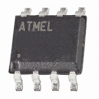
ATTINY13-20SSU Atmel, ATTINY13-20SSU Datasheet - Page 101

ATTINY13-20SSU
Manufacturer Part Number
ATTINY13-20SSU
Description
IC MCU AVR 1K FLASH 20MHZ 8SOIC
Manufacturer
Atmel
Series
AVR® ATtinyr
Specifications of ATTINY13-20SSU
Core Processor
AVR
Core Size
8-Bit
Speed
20MHz
Peripherals
Brown-out Detect/Reset, POR, PWM, WDT
Number Of I /o
6
Program Memory Size
1KB (512 x 16)
Program Memory Type
FLASH
Eeprom Size
64 x 8
Ram Size
64 x 8
Voltage - Supply (vcc/vdd)
2.7 V ~ 5.5 V
Data Converters
A/D 4x10b
Oscillator Type
Internal
Operating Temperature
-40°C ~ 85°C
Package / Case
8-SOIC (3.9mm Width)
For Use With
ATSTK600-DIP40 - STK600 SOCKET/ADAPTER 40-PDIP770-1007 - ISP 4PORT ATMEL AVR MCU SPI/JTAGATAVRDRAGON - KIT DRAGON 32KB FLASH MEM AVRATAVRISP2 - PROGRAMMER AVR IN SYSTEMATJTAGICE2 - AVR ON-CHIP D-BUG SYSTEM
Lead Free Status / RoHS Status
Lead free / RoHS Compliant
Connectivity
-
Available stocks
Company
Part Number
Manufacturer
Quantity
Price
Company:
Part Number:
ATTINY13-20SSU-SL383
Manufacturer:
ATMEL
Quantity:
4 132
16.9
16.9.1
2535J–AVR–08/10
Register Description
SPMCSR – Store Program Memory Control and Status Register
The Store Program Memory Control and Status Register contains the control bits needed to con-
trol the Program memory operations.
• Bits 7..5 – Res: Reserved Bits
These bits are reserved bits in the ATtiny13 and always read as zero.
• Bit 4 – CTPB: Clear Temporary Page Buffer
If the CTPB bit is written while filling the temporary page buffer, the temporary page buffer will be
cleared and the data will be lost.
• Bit 3 – RFLB: Read Fuse and Lock Bits
An LPM instruction within three cycles after RFLB and SELFPRGEN are set in the SPMCSR
Register, will read either the lock bits or the fuse bits (depending on Z0 in the Z-pointer) into the
destination register. See
• Bit 2 – PGWRT: Page Write
If this bit is written to one at the same time as SELFPRGEN, the next SPM instruction within four
clock cycles executes Page Write, with the data stored in the temporary buffer. The page
address is taken from the high part of the Z-pointer. The data in R1 and R0 are ignored. The
PGWRT bit will auto-clear upon completion of a Page Write, or if no SPM instruction is executed
within four clock cycles. The CPU is halted during the entire Page Write operation.
• Bit 1 – PGERS: Page Erase
If this bit is written to one at the same time as SELFPRGEN, the next SPM instruction within four
clock cycles executes Page Erase. The page address is taken from the high part of the Z-
pointer. The data in R1 and R0 are ignored. The PGERS bit will auto-clear upon completion of a
Page Erase, or if no SPM instruction is executed within four clock cycles. The CPU is halted dur-
ing the entire Page Write operation.
• Bit 0 – SELFPRGEN: Self Programming Enable
This bit enables the SPM instruction for the next four clock cycles. If written to one together with
either CTPB, RFLB, PGWRT, or PGERS, the following SPM instruction will have a special
meaning, see description above. If only SELFPRGEN is written, the following SPM instruction
will store the value in R1:R0 in the temporary page buffer addressed by the Z-pointer. The LSB
of the Z-pointer is ignored. The SELFPRGEN bit will auto-clear upon completion of an SPM
instruction, or if no SPM instruction is executed within four clock cycles. During Page Erase and
Page Write, the SELFPRGEN bit remains high until the operation is completed.
Writing any other combination than “10001”, “01001”, “00101”, “00011” or “00001” in the lower
five bits will have no effect.
Bit
Read/Write
Initial Value
R
7
–
0
“EEPROM Write Prevents Writing to SPMCSR” on page 99
R
6
0
–
R
5
–
0
CTPB
R/W
4
0
RFLB
R/W
3
0
PGWRT
R/W
2
0
PGERS
R/W
1
0
SELFPRGEN
R/W
0
0
for details.
SPMCSR
101


