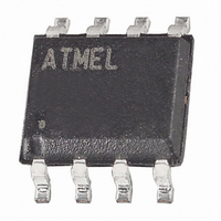
ATTINY13-20SSU Atmel, ATTINY13-20SSU Datasheet - Page 73

ATTINY13-20SSU
Manufacturer Part Number
ATTINY13-20SSU
Description
IC MCU AVR 1K FLASH 20MHZ 8SOIC
Manufacturer
Atmel
Series
AVR® ATtinyr
Specifications of ATTINY13-20SSU
Core Processor
AVR
Core Size
8-Bit
Speed
20MHz
Peripherals
Brown-out Detect/Reset, POR, PWM, WDT
Number Of I /o
6
Program Memory Size
1KB (512 x 16)
Program Memory Type
FLASH
Eeprom Size
64 x 8
Ram Size
64 x 8
Voltage - Supply (vcc/vdd)
2.7 V ~ 5.5 V
Data Converters
A/D 4x10b
Oscillator Type
Internal
Operating Temperature
-40°C ~ 85°C
Package / Case
8-SOIC (3.9mm Width)
For Use With
ATSTK600-DIP40 - STK600 SOCKET/ADAPTER 40-PDIP770-1007 - ISP 4PORT ATMEL AVR MCU SPI/JTAGATAVRDRAGON - KIT DRAGON 32KB FLASH MEM AVRATAVRISP2 - PROGRAMMER AVR IN SYSTEMATJTAGICE2 - AVR ON-CHIP D-BUG SYSTEM
Lead Free Status / RoHS Status
Lead free / RoHS Compliant
Connectivity
-
Available stocks
Company
Part Number
Manufacturer
Quantity
Price
Company:
Part Number:
ATTINY13-20SSU-SL383
Manufacturer:
ATMEL
Quantity:
4 132
11.9.3
2535J–AVR–08/10
TCNT0 – Timer/Counter Register
• Bit 6 – FOC0B: Force Output Compare B
The FOC0B bit is only active when the WGM bits specify a non-PWM mode.
However, for ensuring compatibility with future devices, this bit must be set to zero when
TCCR0B is written when operating in PWM mode. When writing a logical one to the FOC0B bit,
an immediate Compare Match is forced on the Waveform Generation unit. The OC0B output is
changed according to its COM0B1:0 bits setting. Note that the FOC0B bit is implemented as a
strobe. Therefore it is the value present in the COM0B1:0 bits that determines the effect of the
forced compare.
A FOC0B strobe will not generate any interrupt, nor will it clear the timer in CTC mode using
OCR0B as TOP.
The FOC0B bit is always read as zero.
• Bits 5:4 – Res: Reserved Bits
These bits are reserved bits in the ATtiny13 and will always read as zero.
• Bit 3 – WGM02: Waveform Generation Mode
See the description in the
• Bits 2:0 – CS02:0: Clock Select
The three Clock Select bits select the clock source to be used by the Timer/Counter.
Table 11-9.
If external pin modes are used for the Timer/Counter0, transitions on the T0 pin will clock the
counter even if the pin is configured as an output. This feature allows software control of the
counting.
The Timer/Counter Register gives direct access, both for read and write operations, to the
Timer/Counter unit 8-bit counter. Writing to the TCNT0 Register blocks (removes) the Compare
Match on the following timer clock. Modifying the counter (TCNT0) while the counter is running,
introduces a risk of missing a Compare Match between TCNT0 and the OCR0x Registers.
Bit
Read/Write
Initial Value
CS02
0
0
0
0
1
1
1
1
CS01
0
0
1
1
0
0
1
1
Clock Select Bit Description
R/W
7
0
CS00
0
1
0
1
0
1
0
1
R/W
“TCCR0A – Timer/Counter Control Register A” on page
6
0
Description
No clock source (Timer/Counter stopped)
clk
clk
clk
clk
clk
External clock source on T0 pin. Clock on falling edge.
External clock source on T0 pin. Clock on rising edge.
I/O
I/O
I/O
I/O
I/O
/(No prescaling)
/8 (From prescaler)
/64 (From prescaler)
/256 (From prescaler)
/1024 (From prescaler)
R/W
5
0
R/W
4
0
TCNT0[7:0]
R/W
3
0
R/W
2
0
R/W
1
0
R/W
0
0
69.
TCNT0
73


