ATTINY24-20PU Atmel, ATTINY24-20PU Datasheet - Page 110
ATTINY24-20PU
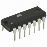
Manufacturer Part Number
ATTINY24-20PU
Description
IC MCU AVR 2K FLASH 20MHZ 14-DIP
Manufacturer
Atmel
Series
AVR® ATtinyr
Specifications of ATTINY24-20PU
Core Processor
AVR
Core Size
8-Bit
Speed
20MHz
Connectivity
USI
Peripherals
Brown-out Detect/Reset, POR, PWM, Temp Sensor, WDT
Number Of I /o
12
Program Memory Size
2KB (1K x 16)
Program Memory Type
FLASH
Eeprom Size
128 x 8
Ram Size
128 x 8
Voltage - Supply (vcc/vdd)
2.7 V ~ 5.5 V
Data Converters
A/D 8x10b
Oscillator Type
Internal
Operating Temperature
-40°C ~ 85°C
Package / Case
14-DIP (0.300", 7.62mm)
Processor Series
ATTINY2x
Core
AVR8
Data Bus Width
8 bit
Data Ram Size
128 B
Interface Type
SPI
Maximum Clock Frequency
20 MHz
Number Of Programmable I/os
12
Number Of Timers
2
Operating Supply Voltage
2.7 V to 5.5 V
Maximum Operating Temperature
+ 85 C
Mounting Style
Through Hole
3rd Party Development Tools
EWAVR, EWAVR-BL
Development Tools By Supplier
ATAVRDRAGON, ATSTK500, ATSTK600, ATAVRISP2, ATAVRONEKIT
Minimum Operating Temperature
- 40 C
On-chip Adc
8-ch x 10-bit
For Use With
ATSTK600-DIP40 - STK600 SOCKET/ADAPTER 40-PDIP770-1007 - ISP 4PORT ATMEL AVR MCU SPI/JTAGATAVRISP2 - PROGRAMMER AVR IN SYSTEMATSTK505 - ADAPTER KIT FOR 14PIN AVR MCU
Lead Free Status / RoHS Status
Lead free / RoHS Compliant


12.11.2
110
ATtiny24/44/84
TCCR1B – Timer/Counter1 Control Register B
• Bits 1:0 – WGM11, WGM10: Waveform Generation Mode
Combined with the WGM13:2 bits found in the TCCR1B Register, these bits control the counting
sequence of the counter, the source for maximum (TOP) counter value, and what type of wave-
form generation to be used, see
Timer/Counter unit are: Normal mode (counter), Clear Timer on Compare match (CTC) mode,
and three types of Pulse Width Modulation (PWM) modes.
Table 12-5.
• Bit 7 – ICNC1: Input Capture Noise Canceler
Setting this bit (to one) activates the Input Capture Noise Canceler. When the noise canceler is
activated, the input from the Input Capture pin (ICP1) is filtered. The filter function requires four
successive equal valued samples of the ICP1 pin for changing its output. The Input Capture is
therefore delayed by four Oscillator cycles when the noise canceler is enabled.
• Bit 6 – ICES1: Input Capture Edge Select
This bit selects which edge on the Input Capture pin (ICP1) that is used to trigger a capture
event. When the ICES1 bit is written to zero, a falling (negative) edge is used as trigger, and
when the ICES1 bit is written to one, a rising (positive) edge will trigger the capture.
Bit
0x2E (0x4E)
Read/Write
Initial Value
Mode
10
11
12
13
14
15
0
1
2
3
4
5
6
7
8
9
WGM
13:10
0000
0001
0010
0011
0100
0101
0110
0111
1000
1001
1010
1011
1100
1101
1110
1111
Waveform Generation Modes
ICNC1
R/W
7
0
Mode of
Operation
Normal
PWM, Phase Correct, 8-bit
PWM, Phase Correct, 9-bit
PWM, Phase Correct, 10-bit
CTC (
Fast PWM, 8-bit
Fast PWM, 9-bit
Fast PWM, 10-bit
PWM, Phase & Freq. Correct
PWM, Phase & Freq. Correct
PWM, Phase Correct
PWM, Phase Correct
CTC (
(Reserved)
Fast PWM
Fast PWM
ICES1
R/W
Clear Timer on Compare
Clear Timer on Compare
6
0
Table 12-5 on page
R
5
–
0
WGM13
R/W
4
0
)
)
WGM12
R/W
110. Modes of operation supported by the
3
0
TOP
0xFFFF
0x00FF
0x01FF
0x03FF
OCR1A
0x00FF
0x01FF
0x03FF
ICR1
OCR1A
ICR1
OCR1A
ICR1
–
ICR1
OCR1A
(“Modes of Operation” on page
CS12
R/W
2
0
Update of
OCR1
Immediate
TOP
TOP
TOP
Immediate
TOP
TOP
TOP
BOTTOM
BOTTOM
TOP
TOP
Immediate
–
TOP
TOP
CS11
R/W
1
0
x
at
CS10
R/W
0
0
TOV1 Flag
Set on
MAX
BOTTOM
BOTTOM
BOTTOM
MAX
TOP
TOP
TOP
BOTTOM
BOTTOM
BOTTOM
BOTTOM
MAX
–
TOP
TOP
8006K–AVR–10/10
TCCR1B
96).
Related parts for ATTINY24-20PU
Image
Part Number
Description
Manufacturer
Datasheet
Request
R

Part Number:
Description:
Manufacturer:
Atmel Corporation
Datasheet:
Part Number:
Description:
Manufacturer:
Atmel Corporation
Datasheet:

Part Number:
Description:
IC MCU AVR 2K FLASH 20MHZ 20-QFN
Manufacturer:
Atmel
Datasheet:

Part Number:
Description:
IC MCU AVR 2K FLASH 20MHZ 14SOIC
Manufacturer:
Atmel
Datasheet:

Part Number:
Description:
MCU AVR 2K FLASH 15MHZ 20-QFN
Manufacturer:
Atmel
Datasheet:

Part Number:
Description:
MCU AVR 2KB FLASH 20MHZ 14SOIC
Manufacturer:
Atmel
Datasheet:
Part Number:
Description:
MCU AVR 2KB FLASH 20MHZ 20QFN
Manufacturer:
Atmel
Datasheet:
Part Number:
Description:
MCU AVR 2K FLASH 15MHZ 14-SOIC
Manufacturer:
Atmel
Datasheet:

Part Number:
Description:
DEV KIT FOR AVR/AVR32
Manufacturer:
Atmel
Datasheet:
Part Number:
Description:
INTERVAL AND WIPE/WASH WIPER CONTROL IC WITH DELAY
Manufacturer:
ATMEL Corporation
Datasheet:
Part Number:
Description:
Low-Voltage Voice-Switched IC for Hands-Free Operation
Manufacturer:
ATMEL Corporation
Datasheet:
Part Number:
Description:
MONOLITHIC INTEGRATED FEATUREPHONE CIRCUIT
Manufacturer:
ATMEL Corporation
Datasheet: