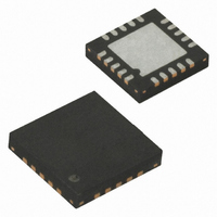
ATTINY84-20MU Atmel, ATTINY84-20MU Datasheet - Page 102

ATTINY84-20MU
Manufacturer Part Number
ATTINY84-20MU
Description
IC MCU AVR 8K FLASH 20MHZ 20-QFN
Manufacturer
Atmel
Series
AVR® ATtinyr
Specifications of ATTINY84-20MU
Core Processor
AVR
Core Size
8-Bit
Speed
20MHz
Connectivity
USI
Peripherals
Brown-out Detect/Reset, POR, PWM, Temp Sensor, WDT
Number Of I /o
12
Program Memory Size
8KB (4K x 16)
Program Memory Type
FLASH
Eeprom Size
512 x 8
Ram Size
512 x 8
Voltage - Supply (vcc/vdd)
2.7 V ~ 5.5 V
Data Converters
A/D 8x10b
Oscillator Type
Internal
Operating Temperature
-40°C ~ 85°C
Package / Case
20-MLF®, QFN
Cpu Family
ATtiny
Device Core
AVR
Device Core Size
8b
Frequency (max)
20MHz
Interface Type
SPI/USI
Total Internal Ram Size
512Byte
# I/os (max)
12
Number Of Timers - General Purpose
2
Operating Supply Voltage (typ)
3.3/5V
Operating Supply Voltage (max)
5.5V
Operating Supply Voltage (min)
2.7V
On-chip Adc
8-chx10-bit
Instruction Set Architecture
RISC
Operating Temp Range
-40C to 85C
Operating Temperature Classification
Industrial
Mounting
Surface Mount
Pin Count
20
Package Type
MLF
Processor Series
ATTINY8x
Core
AVR8
Data Bus Width
8 bit
Data Ram Size
512 B
Maximum Clock Frequency
20 MHz
Number Of Programmable I/os
12
Number Of Timers
2
Operating Supply Voltage
2.7 V to 5.5 V
Maximum Operating Temperature
+ 85 C
Mounting Style
SMD/SMT
3rd Party Development Tools
EWAVR, EWAVR-BL
Development Tools By Supplier
ATAVRDRAGON, ATSTK500, ATSTK600, ATAVRISP2, ATAVRONEKIT
Minimum Operating Temperature
- 40 C
Package
20MLF
Family Name
ATtiny
Maximum Speed
20 MHz
For Use With
ATSTK600 - DEV KIT FOR AVR/AVR32770-1007 - ISP 4PORT ATMEL AVR MCU SPI/JTAGATAVRISP2 - PROGRAMMER AVR IN SYSTEM
Lead Free Status / RoHS Status
Lead free / RoHS Compliant
Available stocks
Company
Part Number
Manufacturer
Quantity
Price
102
ATtiny24/44/84
the maximum resolution is 16-bit (ICR1 or OCR1A set to MAX). The PWM resolution in bits can
be calculated using the following equation:
In phase and frequency correct PWM mode the counter is incremented until the counter value
matches either the value in ICR1 (WGM13:0 = 8), or the value in OCR1A (WGM13:0 = 9). The
counter has then reached the TOP and changes the count direction. The TCNT1 value will be
equal to TOP for one timer clock cycle. The timing diagram for the phase correct and frequency
correct PWM mode is shown on
quency correct PWM mode when OCR1A or ICR1 is used to define TOP. The TCNT1 value is in
the timing diagram shown as a histogram for illustrating the dual-slope operation. The diagram
includes non-inverted and inverted PWM outputs. The small horizontal line marks on the TCNT1
slopes represent compare matches between OCR1x and TCNT1. The OC1x interrupt flag will be
set when a compare match occurs.
Figure 12-9. Phase and Frequency Correct PWM Mode, Timing Diagram
The Timer/Counter Overflow Flag (TOV1) is set at the same timer clock cycle as the OCR1x
Registers are updated with the double buffer value (at BOTTOM). When either OCR1A or ICR1
is used for defining the TOP value, the OC1A or ICF1 flag set when TCNT1 has reached TOP.
The interrupt flags can then be used to generate an interrupt each time the counter reaches the
TOP or BOTTOM value.
When changing the TOP value the program must ensure that the new TOP value is higher or
equal to the value of all of the Compare Registers. If the TOP value is lower than any of the
Compare Registers, a compare match will never occur between the TCNT1 and the OCR1x.
As
mode, symmetrical in all periods. Since the OCR1x Registers are updated at BOTTOM, the
length of the rising and the falling slopes will always be equal. This gives symmetrical output
pulses and is therefore frequency correct.
TCNTn
OCnx
OCnx
Period
Figure 12-9 on page 102
1
shows the output generated is, in contrast to the phase correct
Figure 12-9 on page
R
PFCPWM
2
=
3
log
---------------------------------- -
(
log
TOP
2 ( )
102. The figure shows phase and fre-
+
1
)
4
OCnA Interrupt Flag Set
or ICFn Interrupt Flag Set
(Interrupt on TOP)
(COMnx1:0 = 2)
(COMnx1:0 = 3)
OCRnx/TOP Updateand
TOVn Interrupt Flag Set
(Interrupt on Bottom)
8006K–AVR–10/10


