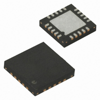
ATTINY84-20MU Atmel, ATTINY84-20MU Datasheet - Page 62

ATTINY84-20MU
Manufacturer Part Number
ATTINY84-20MU
Description
IC MCU AVR 8K FLASH 20MHZ 20-QFN
Manufacturer
Atmel
Series
AVR® ATtinyr
Specifications of ATTINY84-20MU
Core Processor
AVR
Core Size
8-Bit
Speed
20MHz
Connectivity
USI
Peripherals
Brown-out Detect/Reset, POR, PWM, Temp Sensor, WDT
Number Of I /o
12
Program Memory Size
8KB (4K x 16)
Program Memory Type
FLASH
Eeprom Size
512 x 8
Ram Size
512 x 8
Voltage - Supply (vcc/vdd)
2.7 V ~ 5.5 V
Data Converters
A/D 8x10b
Oscillator Type
Internal
Operating Temperature
-40°C ~ 85°C
Package / Case
20-MLF®, QFN
Cpu Family
ATtiny
Device Core
AVR
Device Core Size
8b
Frequency (max)
20MHz
Interface Type
SPI/USI
Total Internal Ram Size
512Byte
# I/os (max)
12
Number Of Timers - General Purpose
2
Operating Supply Voltage (typ)
3.3/5V
Operating Supply Voltage (max)
5.5V
Operating Supply Voltage (min)
2.7V
On-chip Adc
8-chx10-bit
Instruction Set Architecture
RISC
Operating Temp Range
-40C to 85C
Operating Temperature Classification
Industrial
Mounting
Surface Mount
Pin Count
20
Package Type
MLF
Processor Series
ATTINY8x
Core
AVR8
Data Bus Width
8 bit
Data Ram Size
512 B
Maximum Clock Frequency
20 MHz
Number Of Programmable I/os
12
Number Of Timers
2
Operating Supply Voltage
2.7 V to 5.5 V
Maximum Operating Temperature
+ 85 C
Mounting Style
SMD/SMT
3rd Party Development Tools
EWAVR, EWAVR-BL
Development Tools By Supplier
ATAVRDRAGON, ATSTK500, ATSTK600, ATAVRISP2, ATAVRONEKIT
Minimum Operating Temperature
- 40 C
Package
20MLF
Family Name
ATtiny
Maximum Speed
20 MHz
For Use With
ATSTK600 - DEV KIT FOR AVR/AVR32770-1007 - ISP 4PORT ATMEL AVR MCU SPI/JTAGATAVRISP2 - PROGRAMMER AVR IN SYSTEM
Lead Free Status / RoHS Status
Lead free / RoHS Compliant
Available stocks
Company
Part Number
Manufacturer
Quantity
Price
62
ATtiny24/44/84
• Port A, Bit 1 – ADC1/AIN0/PCINT1
• Port A, Bit 2 – ADC2/AIN1/PCINT2
• Port A, Bit 3 – ADC3/T0/PCINT3
• Port A, Bit 4 – ADC4/USCK/SCL/T1/PCINT4
• Port A, Bit 5 – ADC5/DO/MISO/OC1B/PCINT5
• ADC1: Analog to Digital Converter, Channel 1
• AIN0: Analog Comparator Positive Input. Configure the port pin as input with the internal pull-
• PCINT1: Pin Change Interrupt source 1. The PA1 pin can serve as an external interrupt
• ADC2: Analog to Digital Converter, Channel 2
• AIN1: Analog Comparator Negative Input. Configure the port pin as input with the internal
• PCINT2: Pin Change Interrupt source 2. The PA2 pin can serve as an external interrupt
• ADC3: Analog to Digital Converter, Channel 3
• T0: Timer/Counter0 counter source.
• PCINT3: Pin Change Interrupt source 3. The PA3 pin can serve as an external interrupt
• ADC4: Analog to Digital Converter, Channel 4
• USCK: Three-wire mode Universal Serial Interface Clock.
• SCL: Two-wire mode Serial Clock for USI Two-wire mode.
• T1: Timer/Counter1 counter source.
• PCINT4: Pin Change Interrupt source 4. The PA4 pin can serve as an external interrupt
• ADC5: Analog to Digital Converter, Channel 5
• DO: Data Output in USI Three-wire mode. Data output (DO) overrides PORTA5 value and it
• MISO: Master Data input, Slave Data output pin for SPI channel. When the SPI is enabled as
• OC1B: Output Compare Match output: The PA5 pin can serve as an external output for the
• PCINT5: Pin Change Interrupt source 5. The PA5 pin can serve as an external interrupt
up switched off to avoid the digital port function from interfering with the function of the
Analog Comparator.
source for pin change interrupt 0.
pull-up switched off to avoid the digital port function from interfering with the function of the
Analog Comparator.
source for pin change interrupt 0.
source for pin change interrupt 0.
source for pin change interrupt 0.
is driven to the port when the data direction bit DDA5 is set (one). However the PORTA5 bit
still controls the pullup, enabling pullup if direction is input and PORTA5 is set(one).
a Master, this pin is configured as an input regardless of the setting of DDA5. When the SPI is
enabled as a Slave, the data direction of this pin is controlled by DDA5. When the pin is
forced by the SPI to be an input, the pull-up can still be controlled by the PORTA5 bit.
Timer/Counter1 Compare Match B. The PA5 pin has to be configured as an output (DDA5 set
(one)) to serve this function. The OC1B pin is also the output pin for the PWM mode timer
function.
source for pin change interrupt 0.
.
.
.
.
.
8006K–AVR–10/10


