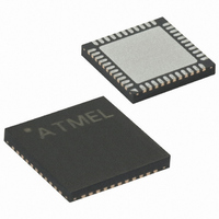
ATMEGA32A-MU Atmel, ATMEGA32A-MU Datasheet - Page 114

ATMEGA32A-MU
Manufacturer Part Number
ATMEGA32A-MU
Description
MCU AVR 32K FLASH 16MHZ 44-QFN
Manufacturer
Atmel
Series
AVR® ATmegar
Specifications of ATMEGA32A-MU
Core Processor
AVR
Core Size
8-Bit
Speed
16MHz
Connectivity
I²C, SPI, UART/USART
Peripherals
Brown-out Detect/Reset, POR, PWM, WDT
Number Of I /o
32
Program Memory Size
32KB (16K x 16)
Program Memory Type
FLASH
Eeprom Size
1K x 8
Ram Size
2K x 8
Voltage - Supply (vcc/vdd)
2.7 V ~ 5.5 V
Data Converters
A/D 8x10b
Oscillator Type
Internal
Operating Temperature
-40°C ~ 85°C
Package / Case
44-VQFN Exposed Pad
Processor Series
ATMEGA32x
Core
AVR8
Data Bus Width
8 bit
Data Ram Size
2 KB
Interface Type
2-Wire, SPI, USART
Maximum Clock Frequency
16 MHz
Number Of Programmable I/os
32
Number Of Timers
3
Maximum Operating Temperature
+ 85 C
Mounting Style
SMD/SMT
3rd Party Development Tools
EWAVR, EWAVR-BL
Development Tools By Supplier
ATAVRDRAGON, ATSTK500, ATSTK600, ATAVRISP2, ATAVRONEKIT
Minimum Operating Temperature
- 40 C
On-chip Adc
10 bit, 8 Channel
Controller Family/series
AVR MEGA
No. Of I/o's
32
Eeprom Memory Size
1KB
Ram Memory Size
2KB
Cpu Speed
16MHz
Rohs Compliant
Yes
For Use With
ATSTK524 - KIT STARTER ATMEGA32M1/MEGA32C1ATSTK600 - DEV KIT FOR AVR/AVR32ATAVRDRAGON - KIT DRAGON 32KB FLASH MEM AVRATSTK500 - PROGRAMMER AVR STARTER KIT
Lead Free Status / RoHS Status
Lead free / RoHS Compliant
Available stocks
Company
Part Number
Manufacturer
Quantity
Price
Part Number:
ATMEGA32A-MU
Manufacturer:
MICROCHIP/微芯
Quantity:
20 000
- Current page: 114 of 353
- Download datasheet (6Mb)
Table 16-5.
Note:
16.10.2
8155C–AVR–02/11
Mode
10
11
12
13
14
15
0
1
2
3
4
5
6
7
8
9
1. The CTC1 and PWM11:0 bit definition names are obsolete. Use the
WGM13
TCCR1B – Timer/Counter1 Control Register B
location of these bits are compatible with previous versions of the timer.
0
0
0
0
0
0
0
0
1
1
1
1
1
1
1
1
Waveform Generation Mode Bit Description
WGM12
(CTC1)
0
0
0
0
1
1
1
1
0
0
0
0
1
1
1
1
TCCR1A is written when operating in a PWM mode. When writing a logical one to the
FOC1A/FOC1B bit, an immediate compare match is forced on the Waveform Generation unit.
The OC1A/OC1B output is changed according to its COM1x1:0 bits setting. Note that the
FOC1A/FOC1B bits are implemented as strobes. Therefore it is the value present in the
COM1x1:0 bits that determine the effect of the forced compare.
A FOC1A/FOC1B strobe will not generate any interrupt nor will it clear the timer in Clear Timer
on Compare match (CTC) mode using OCR1A as TOP.
The FOC1A/FOC1B bits are always read as zero.
• Bit 1:0 – WGM11:0: Waveform Generation Mode
Combined with the WGM13:2 bits found in the TCCR1B Register, these bits control the counting
sequence of the counter, the source for maximum (TOP) counter value, and what type of wave-
form generation to be used, see
unit are: Normal mode (counter), Clear Timer on Compare match (CTC) mode, and three types
of Pulse Width Modulation (PWM) modes.
Bit
Read/Write
Initial Value
(PWM11)
WGM11
0
0
1
1
0
0
1
1
0
0
1
1
0
0
1
1
(PWM10)
WGM10
ICNC1
R/W
7
0
0
1
0
1
0
1
0
1
0
1
0
1
0
1
0
1
ICES1
R/W
Timer/Counter Mode of
Operation
Normal
PWM, Phase Correct, 8-bit
PWM, Phase Correct, 9-bit
PWM, Phase Correct, 10-bit
CTC
Fast PWM, 8-bit
Fast PWM, 9-bit
Fast PWM, 10-bit
PWM, Phase and Frequency Correct
PWM, Phase and Frequency Correct
PWM, Phase Correct
PWM, Phase Correct
CTC
Reserved
Fast PWM
Fast PWM
6
0
(1)
Table
R
5
–
0
16-5. Modes of operation supported by the Timer/Counter
WGM13
(See “Modes of Operation” on page
R/W
4
0
WGM
WGM12
12:0 definitions. However, the functionality and
R/W
3
0
TOP
0xFFFF
0x00FF
0x01FF
0x03FF
OCR1A
0x00FF
0x01FF
0x03FF
ICR1
OCR1A
ICR1
OCR1A
ICR1
–
ICR1
OCR1A
CS12
R/W
2
0
Update of
OCR1
TOP
–
BOTTOM
Immediate
TOP
TOP
TOP
Immediate
BOTTOM
BOTTOM
BOTTOM
BOTTOM
BOTTOM
TOP
Immediate
BOTTOM
CS11
R/W
1
0
ATmega32A
x
103.)
CS10
R/W
0
0
TOV1 Flag Set
on
MAX
BOTTOM
BOTTOM
BOTTOM
MAX
TOP
TOP
TOP
BOTTOM
BOTTOM
BOTTOM
BOTTOM
MAX
–
TOP
TOP
TCCR1B
114
Related parts for ATMEGA32A-MU
Image
Part Number
Description
Manufacturer
Datasheet
Request
R

Part Number:
Description:
Manufacturer:
Atmel Corporation
Datasheet:

Part Number:
Description:
Manufacturer:
ATMEL Corporation
Datasheet:

Part Number:
Description:
IC AVR MCU 32K 16MHZ 5V 44-QFN
Manufacturer:
Atmel
Datasheet:

Part Number:
Description:
IC AVR MCU 32K 16MHZ 5V 40DIP
Manufacturer:
Atmel
Datasheet:

Part Number:
Description:
IC AVR MCU 32K 16MHZ 5V 44TQFP
Manufacturer:
Atmel
Datasheet:

Part Number:
Description:
IC AVR MCU 32K 16MHZ IND 40-DIP
Manufacturer:
Atmel
Datasheet:

Part Number:
Description:
IC AVR MCU 32K 16MHZ IND 44-TQFP
Manufacturer:
Atmel
Datasheet:

Part Number:
Description:
MCU AVR 32KB FLASH 16MHZ 44TQFP
Manufacturer:
Atmel
Datasheet:

Part Number:
Description:
MCU AVR 32KB FLASH 16MHZ 44QFN
Manufacturer:
Atmel
Datasheet:

Part Number:
Description:
MCU AVR 32K FLASH 16MHZ 44-TQFP
Manufacturer:
Atmel
Datasheet:

Part Number:
Description:
IC AVR MCU 32K 16MHZ COM 40-DIP
Manufacturer:
Atmel
Datasheet:

Part Number:
Description:
IC AVR MCU 32K 16MHZ COM 44-QFN
Manufacturer:
Atmel
Datasheet:

Part Number:
Description:
IC AVR MCU 32K 16MHZ COM 44-TQFP
Manufacturer:
Atmel
Datasheet:


