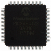
PIC24FJ128GA010-I/PT Microchip Technology, PIC24FJ128GA010-I/PT Datasheet - Page 99

PIC24FJ128GA010-I/PT
Manufacturer Part Number
PIC24FJ128GA010-I/PT
Description
IC PIC MCU FLASH 128K 100TQFP
Manufacturer
Microchip Technology
Series
PIC® 24Fr
Datasheets
1.PIC24FJ16GA002-ISS.pdf
(52 pages)
2.PIC24FJ64GA006-IPT.pdf
(240 pages)
3.PIC24FJ64GA006-IPT.pdf
(22 pages)
4.PIC24FJ128GA008-IPT.pdf
(12 pages)
5.PIC24FJ128GA006-IPT.pdf
(231 pages)
6.PIC24FJ128GA010-IPT.pdf
(230 pages)
Specifications of PIC24FJ128GA010-I/PT
Core Size
16-Bit
Program Memory Size
128KB (43K x 24)
Core Processor
PIC
Speed
16MHz
Connectivity
I²C, PMP, SPI, UART/USART
Peripherals
Brown-out Detect/Reset, POR, PWM, WDT
Number Of I /o
84
Program Memory Type
FLASH
Ram Size
8K x 8
Voltage - Supply (vcc/vdd)
2 V ~ 3.6 V
Data Converters
A/D 16x10b
Oscillator Type
Internal
Operating Temperature
-40°C ~ 85°C
Package / Case
100-TFQFP
Controller Family/series
PIC24
No. Of I/o's
84
Ram Memory Size
8KB
Cpu Speed
32MHz
No. Of Timers
5
No. Of Pwm Channels
5
Embedded Interface Type
EUART, I2C, PSP, SPI
Rohs Compliant
Yes
Processor Series
PIC24FJ
Core
PIC
Data Bus Width
16 bit
Data Ram Size
8 KB
Interface Type
SPI, I2C, USART
Maximum Clock Frequency
16 MHz
Number Of Programmable I/os
54
Number Of Timers
5
Maximum Operating Temperature
+ 85 C
Mounting Style
SMD/SMT
3rd Party Development Tools
52713-733, 52714-737, 53276-922, EWDSPIC
Development Tools By Supplier
PG164130, DV164035, DV244005, DV164005, PG164120, DM240001, DM240011
Minimum Operating Temperature
- 40 C
On-chip Adc
10 bit, 16 Channel
Package
100TQFP
Device Core
PIC
Family Name
PIC24
Maximum Speed
16 MHz
Operating Supply Voltage
2.5|3.3 V
Lead Free Status / RoHS Status
Lead free / RoHS Compliant
For Use With
DM240011 - KIT STARTER MPLAB FOR PIC24F MCUAC164333 - MODULE SKT FOR PM3 100QFPDV164033 - KIT START EXPLORER 16 MPLAB ICD2MA160011 - DAUGHTER BOARD PICDEM LCD 16F91XDM240001 - BOARD DEMO PIC24/DSPIC33/PIC32
Eeprom Size
-
Lead Free Status / Rohs Status
Details
Available stocks
Company
Part Number
Manufacturer
Quantity
Price
Company:
Part Number:
PIC24FJ128GA010-I/PT
Manufacturer:
Microchi
Quantity:
627
Company:
Part Number:
PIC24FJ128GA010-I/PT
Manufacturer:
MICROCHIP
Quantity:
212
Company:
Part Number:
PIC24FJ128GA010-I/PT
Manufacturer:
Microchip Technology
Quantity:
10 000
7.4
With few limitations, applications are free to switch
between any of the four clock sources (POSC, SOSC,
FRC and LPRC) under software control and at any
time. To limit the possible side effects that could result
from this flexibility, PIC24F devices have a safeguard
lock built into the switching process.
7.4.1
To enable clock switching, the FCKSM1 Configuration bit
in the Flash Configuration Word 2 register must be pro-
grammed to ‘0’. (Refer to Section 23.1 “Configuration
Bits” for further details.) If the FCKSM1 Configuration bit
is unprogrammed (‘1’), the clock switching function and
Fail-Safe Clock Monitor function are disabled. This is the
default setting.
The NOSC control bits (OSCCON<10:8>) do not
control the clock selection when clock switching is dis-
abled. However, the COSC bits (OSCCON<14:12>)
will reflect the clock source selected by the FNOSC
Configuration bits.
The OSWEN control bit (OSCCON<0>) has no effect
when clock switching is disabled. It is held at ‘0’ at all
times.
7.4.2
At a minimum, performing a clock switch requires this
basic sequence:
1.
2.
3.
4.
5.
© 2009 Microchip Technology Inc.
Note:
If
(OSCCON<14:12>), to determine the current
oscillator source.
Perform the unlock sequence to allow a write to
the OSCCON register high byte.
Write the appropriate value to the NOSC control
bits (OSCCON<10:8>) for the new oscillator
source.
Perform the unlock sequence to allow a write to
the OSCCON register low byte.
Set the OSWEN bit to initiate the oscillator
switch.
Clock Switching Operation
desired,
Primary
different submodes (XT, HS and EC)
which are determined by the POSCMD
Configuration bits. While an application
can switch to and from primary oscillator
mode in software, it cannot switch
between the different primary submodes
without reprogramming the device.
ENABLING CLOCK SWITCHING
OSCILLATOR SWITCHING
SEQUENCE
read
oscillator
the
mode
COSC
has
PIC24FJ128GA010 FAMILY
three
bits
Once the basic sequence is completed, the system
clock hardware responds automatically as follows:
1.
2.
3.
4.
5.
6.
Note 1: The processor will continue to execute
The clock switching hardware compares the
COSC status bits with the new value of the
NOSC control bits. If they are the same, then the
clock switch is a redundant operation. In this
case, the OSWEN bit is cleared automatically
and the clock switch is aborted.
If a valid clock switch has been initiated, the
LOCK (OSCCON<5>) and CF (OSCCON<3>)
status bits are cleared.
The new oscillator is turned on by the hardware
if it is not currently running. If a crystal oscillator
must be turned on, the hardware will wait until
the OST expires. If the new source is using the
PLL, then the hardware waits until a PLL lock is
detected (LOCK = 1).
The hardware waits for 10 clock cycles from the
new clock source and then performs the clock
switch.
The hardware clears the OSWEN bit to indicate a
successful clock transition. In addition, the NOSC
bit values are transferred to the COSC status bits.
The old clock source is turned off at this time,
with the exception of LPRC (if WDT or FSCM
are enabled) or SOSC (if SOSCEN remains
set).
2: Direct clock switches between any
code throughout the clock switching
sequence. Timing sensitive code should
not be executed during this time.
primary oscillator mode with PLL and
FRCPLL mode are not permitted. This
applies to clock switches in either direc-
tion. In these instances, the application
must switch to FRC mode as a transition
clock source between the two PLL
modes.
DS39747E-page 99


