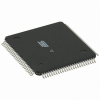
ATMEGA3290PV-10AU Atmel, ATMEGA3290PV-10AU Datasheet - Page 150

ATMEGA3290PV-10AU
Manufacturer Part Number
ATMEGA3290PV-10AU
Description
IC MCU 32K 4X40 LCD CTRL 100TQFP
Manufacturer
Atmel
Series
AVR® ATmegar
Specifications of ATMEGA3290PV-10AU
Core Processor
AVR
Core Size
8-Bit
Speed
10MHz
Connectivity
SPI, UART/USART, USI
Peripherals
Brown-out Detect/Reset, LCD, POR, PWM, WDT
Number Of I /o
69
Program Memory Size
32KB (16K x 16)
Program Memory Type
FLASH
Eeprom Size
1K x 8
Ram Size
2K x 8
Voltage - Supply (vcc/vdd)
1.8 V ~ 5.5 V
Data Converters
A/D 8x10b
Oscillator Type
Internal
Operating Temperature
-40°C ~ 85°C
Package / Case
100-TQFP, 100-VQFP
Processor Series
ATMEGA32x
Core
AVR8
Data Bus Width
8 bit
Data Ram Size
2 KB
Interface Type
SPI, USART, USI
Maximum Clock Frequency
10 MHz
Number Of Programmable I/os
69
Number Of Timers
3
Maximum Operating Temperature
+ 85 C
Mounting Style
SMD/SMT
Minimum Operating Temperature
- 40 C
On-chip Adc
10 bit, 8 Channel
For Use With
ATSTK600-TQFP100 - STK600 SOCKET/ADAPTER 100-TQFP770-1007 - ISP 4PORT ATMEL AVR MCU SPI/JTAG770-1005 - ISP 4PORT FOR ATMEL AVR MCU JTAG770-1004 - ISP 4PORT FOR ATMEL AVR MCU SPIATAVRISP2 - PROGRAMMER AVR IN SYSTEMATSTK504 - STARTER KIT AVR EXP MOD 100P LCDATJTAGICE2 - AVR ON-CHIP D-BUG SYSTEM
Lead Free Status / RoHS Status
Lead free / RoHS Compliant
Other names
ATMEGA3290PV-8AU
ATMEGA3290PV-8AU
ATMEGA3290PV-8AU
Available stocks
Company
Part Number
Manufacturer
Quantity
Price
Company:
Part Number:
ATMEGA3290PV-10AU
Manufacturer:
SIPEX
Quantity:
17 600
Part Number:
ATMEGA3290PV-10AU
Manufacturer:
ATMEL/爱特梅尔
Quantity:
20 000
- Current page: 150 of 427
- Download datasheet (9Mb)
17.8
8021G–AVR–03/11
Timer/Counter Timing Diagrams
In phase correct PWM mode, the compare unit allows generation of PWM waveforms on the
OC2A pin. Setting the COM2A1:0 bits to two will produce a non-inverted PWM. An inverted
PWM output can be generated by setting the COM2A1:0 to three (See
The actual OC2A value will only be visible on the port pin if the data direction for the port pin is
set as output. The PWM waveform is generated by clearing (or setting) the OC2A Register at the
compare match between OCR2A and TCNT2 when the counter increments, and setting (or
clearing) the OC2A Register at compare match between OCR2A and TCNT2 when the counter
decrements. The PWM frequency for the output when using phase correct PWM can be calcu-
lated by the following equation:
The N variable represents the prescale factor (1, 8, 32, 64, 128, 256, or 1024).
The extreme values for the OCR2A Register represent special cases when generating a PWM
waveform output in the phase correct PWM mode. If the OCR2A is set equal to BOTTOM, the
output will be continuously low and if set equal to MAX the output will be continuously high for
non-inverted PWM mode. For inverted PWM the output will have the opposite logic values.
At the very start of period 2 in
there is no Compare Match. The point of this transition is to guarantee symmetry around BOT-
TOM. There are two cases that give a transition without Compare Match.
• OCR2A changes its value from MAX, like in
• The timer starts counting from a value higher than the one in OCR2A, and for that reason
The following figures show the Timer/Counter in synchronous mode, and the timer clock (clk
is therefore shown as a clock enable signal. In asynchronous mode, clk
the Timer/Counter Oscillator clock. The figures include information on when Interrupt Flags are
set.
count sequence close to the MAX value in all modes other than phase correct PWM mode.
Figure 17-8. Timer/Counter Timing Diagram, no Prescaling
OCn pin value is the same as the result of a down-counting compare match. To ensure
symmetry around BOTTOM the OCn value at MAX must correspond to the result of an up-
counting Compare Match.
misses the Compare Match and hence the OCn change that would have happened on the way
up.
Figure 17-8
TCNTn
(clk
TOVn
clk
clk
I/O
I/O
Tn
/1)
contains timing data for basic Timer/Counter operation. The figure shows the
MAX - 1
Figure 17-7
f
OCnxPCPWM
MAX
OCn has a transition from high to low even though
Figure
=
----------------- -
N 510
f
17-7. When the OCR2A value is MAX the
clk_I/O
⋅
ATmega329P/3290P
BOTTOM
Table 17-5 on page
I/O
should be replaced by
BOTTOM + 1
156).
150
T2
)
Related parts for ATMEGA3290PV-10AU
Image
Part Number
Description
Manufacturer
Datasheet
Request
R

Part Number:
Description:
Manufacturer:
Atmel Corporation
Datasheet:

Part Number:
Description:
IC AVR MCU 32K 16MHZ 100TQFP
Manufacturer:
Atmel
Datasheet:

Part Number:
Description:
IC AVR MCU 32K 16MHZ 100TQFP
Manufacturer:
Atmel
Datasheet:

Part Number:
Description:
MCU AVR 32K FLASH 16MHZ 64TQFP
Manufacturer:
Atmel
Datasheet:

Part Number:
Description:
Atmega3290 Avr 8-bit Microcontroller With In-system Programmable Flash
Manufacturer:
ATMEL Corporation
Datasheet:

Part Number:
Description:
Manufacturer:
Atmel Corporation
Datasheet:

Part Number:
Description:
IC AVR MCU 32K 16MHZ 64TQFP
Manufacturer:
Atmel
Datasheet:

Part Number:
Description:
IC AVR MCU 32K 16MHZ 64-QFN
Manufacturer:
Atmel
Datasheet:

Part Number:
Description:
IC AVR MCU 32K 16MHZ 64TQFP
Manufacturer:
Atmel
Datasheet:

Part Number:
Description:
IC AVR MCU 32K 16MHZ 64-QFN
Manufacturer:
Atmel
Datasheet:

Part Number:
Description:
MCU AVR 32K FLASH 16MHZ 64TQFP
Manufacturer:
Atmel
Datasheet:

Part Number:
Description:
MCU AVR 32K FLASH 16MHZ 64QFN
Manufacturer:
Atmel
Datasheet:

Part Number:
Description:
DEV KIT FOR AVR/AVR32
Manufacturer:
Atmel
Datasheet:

Part Number:
Description:
INTERVAL AND WIPE/WASH WIPER CONTROL IC WITH DELAY
Manufacturer:
ATMEL Corporation
Datasheet:


