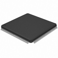
AT91M42800A-33AU Atmel, AT91M42800A-33AU Datasheet - Page 11

AT91M42800A-33AU
Manufacturer Part Number
AT91M42800A-33AU
Description
IC ARM7 MCU 144 LQFP
Manufacturer
Atmel
Series
AT91SAMr
Datasheet
1.AT91M42800A-33AU.pdf
(27 pages)
Specifications of AT91M42800A-33AU
Core Processor
ARM7
Core Size
16/32-Bit
Speed
33MHz
Connectivity
EBI/EMI, SPI, UART/USART
Peripherals
WDT
Number Of I /o
54
Program Memory Type
ROMless
Ram Size
8K x 8
Voltage - Supply (vcc/vdd)
2.7 V ~ 3.6 V
Oscillator Type
External
Operating Temperature
-40°C ~ 85°C
Package / Case
144-LQFP
Processor Series
AT91Mx
Core
ARM7TDMI
Data Bus Width
32 bit
Data Ram Size
8 KB
Interface Type
EBI, SPI, USART
Maximum Clock Frequency
33 MHz
Number Of Programmable I/os
54
Number Of Timers
10 bit
Operating Supply Voltage
3 V to 3.6 V
Maximum Operating Temperature
+ 85 C
Mounting Style
SMD/SMT
3rd Party Development Tools
JTRACE-ARM-2M, MDK-ARM, RL-ARM, ULINK2
Development Tools By Supplier
AT91EB42
Minimum Operating Temperature
- 40 C
For Use With
AT91EB42 - KIT EVAL FOR ARM AT91M42800A
Lead Free Status / RoHS Status
Lead free / RoHS Compliant
Eeprom Size
-
Program Memory Size
-
Data Converters
-
Lead Free Status / Rohs Status
Details
Available stocks
Company
Part Number
Manufacturer
Quantity
Price
Company:
Part Number:
AT91M42800A-33AU
Manufacturer:
Atmel
Quantity:
980
7. Product Overview
7.1
7.2
7.3
7.4
1779ES–ATARM–14-Apr-06
Power Supply
Input/Output Considerations
Operating Modes
Clock Generator
The AT91M42800A has three kinds of power supply pins:
VDDCORE and VDDIO pins allow core power consumption to be reduced by supplying it with a
lower voltage than the I/O lines. The VDDCORE pins must never be powered at a voltage
greater than the supply voltage applied to the VDDIO.
The VDDPLL pin is used to supply the oscillator and both PLLs. The voltage applied on these
pins is typically 3.3V, and it must not be lower than VDDCORE.
Typical supported voltage combinations are shown in the following table:
After the reset, the peripheral I/Os are initialized as inputs to provide the user with maximum
flexibility. It is recommended that in any application phase, the inputs to the AT91M42800A
microcontroller be held at valid logic levels to minimize the power consumption.
The AT91M42800A has two pins dedicated to defining MODE0 and MODE1 operating modes.
These pins allow the user to enter the device in Boundary Scan mode. They also allow the user
to run the processor from the on-chip oscillator and from an external clock by bypassing the on-
chip oscillator. The last mode is reserved for test purposes. A chip reset must be performed
(NRST and NTRST) after MODE0 and/or MODE1 have been changed.
The AT91M42800A microcontroller embeds a 32.768 kHz oscillator that generates the Slow
Clock (SLCK). This on-chip oscillator can be bypassed by setting the correct logical level on
MODE0 and MODE1 pins, as shown above. In this case, SLCK equals XIN.
Pins
VDDCORE
VDDIO
VDDPLL
• VDDCORE pins, which power the chip core
• VDDIO pins, which power the I/O lines
• VDDPLL pins, which power the oscillator and PLL cells
MODE0
0
0
1
1
MODE1
0
1
0
1
Operating Mode
Normal operating mode by using the on-chip oscillator
Boundary Scan Mode
Normal operating mode by using an external clock on XIN
Reserved for test
3.3V
5.0V
3.3V
Nominal Supply Voltages
AT91M42800A
3.0V or 3.3V
3.0V or 3.3V
3.0V or 3.3V
11


