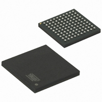
AT91SAM7XC256B-CU Atmel, AT91SAM7XC256B-CU Datasheet - Page 40

AT91SAM7XC256B-CU
Manufacturer Part Number
AT91SAM7XC256B-CU
Description
MCU ARM 256K HS FLASH 100-TFBGA
Manufacturer
Atmel
Series
AT91SAMr
Datasheet
1.AT91SAM7XC128B-CU.pdf
(47 pages)
Specifications of AT91SAM7XC256B-CU
Core Processor
ARM7
Core Size
16/32-Bit
Speed
55MHz
Connectivity
CAN, Ethernet, I²C, SPI, SSC, UART/USART, USB
Peripherals
Brown-out Detect/Reset, DMA, POR, PWM, WDT
Number Of I /o
62
Program Memory Size
256KB (256K x 8)
Program Memory Type
FLASH
Ram Size
64K x 8
Voltage - Supply (vcc/vdd)
1.65 V ~ 1.95 V
Data Converters
A/D 8x10b
Oscillator Type
Internal
Operating Temperature
-40°C ~ 85°C
Package / Case
100-TFBGA
Processor Series
91S
Core
ARM7TDMI
Data Bus Width
32 bit
Data Ram Size
64 KB
Interface Type
CAN, Ethernet, SPI, TWI, USART, USB
Maximum Clock Frequency
55 MHz
Number Of Programmable I/os
62
Number Of Timers
3
Operating Supply Voltage
3.3 V
Maximum Operating Temperature
+ 85 C
Mounting Style
SMD/SMT
Minimum Operating Temperature
- 40 C
Operating Temperature Range
- 40 C to + 85 C
Lead Free Status / RoHS Status
Lead free / RoHS Compliant
Eeprom Size
-
Available stocks
Company
Part Number
Manufacturer
Quantity
Price
10.16 Triple Data Encryption Standard
10.17 Analog-to-Digital Converter
40
AT91SAM7XC512/256/128 Preliminary
• 8-, 16-, 32-, 64- and 128-bit Data Sizes Possible in CFB Mode
• Last Output Data Mode allowing Message Authentication Code (MAC) generation
• Hardware Countermeasures against Differential Power Analysis attacks
• Connection to PDC Channel Capabilities Optimizes Data Transfers for all Operating Modes:
• Single Data Encryption Standard (DES) and Triple Data Encryption
• Algorithm (TDEA or TDES) supports
• Compliant with FIPS Publication 46-3, Data Encryption Standard (DES)
• 64-bit Cryptographic Key
• Two-key or Three-key Algorithms
• 18-clock Cycles Encryption/Decryption Processing Time for DES
• 50-clock Cycles Encryption/Decryption Processing Time for TDES
• Support the Four Standard Modes of Operation specified in the FIPS Publication 81, DES
• Modes of Operation:
• 8-, 16-, 32- and 64- Data Sizes Possible in CFB Mode
• Last Output Data Mode allowing Optimized Message (Data) Authentication Code (MAC)
• Connection to PDC Channel Capabilities Optimizes Data Transfers for all Operating Modes:
• 8-channel ADC
• 10-bit 384 Ksamples/sec. Successive Approximation Register ADC
• ±2 LSB Integral Non Linearity, ±1 LSB Differential Non Linearity
• Integrated 8-to-1 multiplexer, offering eight independent 3.3V analog inputs
• External voltage reference for better accuracy on low voltage inputs
• Individual enable and disable of each channel
• Multiple trigger sources
• Sleep Mode and conversion sequencer
generation
– Counter (CTR)
– One Channel for the Receiver, One Channel for the Transmitter
– Next Buffer Support
– Electronic Codebook (ECB)
– Cipher Block Chaining (CBC)
– Cipher Feedback (CFB)
– Output Feedback (OFB)
– One Channel for the Receiver, One Channel for the Transmitter
– Next Buffer Support
– Hardware or software trigger
– External trigger pin
– Timer Counter 0 to 2 outputs TIOA0 to TIOA2 trigger
6209DS–ATARM–17-Feb-09


