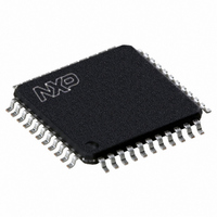
P89LV51RD2BBC,557 NXP Semiconductors, P89LV51RD2BBC,557 Datasheet - Page 8

P89LV51RD2BBC,557
Manufacturer Part Number
P89LV51RD2BBC,557
Description
IC 80C51 MCU FLASH 64K 44-TQFP
Manufacturer
NXP Semiconductors
Series
89LVr
Datasheet
1.P89LV51RD2BBC557.pdf
(76 pages)
Specifications of P89LV51RD2BBC,557
Program Memory Type
FLASH
Program Memory Size
64KB (64K x 8)
Package / Case
44-TQFP, 44-VQFP
Core Processor
8051
Core Size
8-Bit
Speed
33MHz
Connectivity
SPI, UART/USART
Peripherals
Brown-out Detect/Reset, POR, PWM, WDT
Number Of I /o
32
Ram Size
1K x 8
Voltage - Supply (vcc/vdd)
2.7 V ~ 3.6 V
Oscillator Type
Internal
Operating Temperature
0°C ~ 70°C
Processor Series
P89LV5x
Core
80C51
Data Bus Width
8 bit
Data Ram Size
1 KB
Interface Type
SPI/UART
Maximum Clock Frequency
40 MHz
Number Of Programmable I/os
32
Number Of Timers
3
Operating Supply Voltage
2.7 V to 3.6 V
Maximum Operating Temperature
+ 70 C
Mounting Style
SMD/SMT
3rd Party Development Tools
PK51, CA51, A51, ULINK2
Minimum Operating Temperature
0 C
Cpu Family
89LV
Device Core
80C51
Device Core Size
8b
Frequency (max)
40MHz
Total Internal Ram Size
1KB
# I/os (max)
32
Number Of Timers - General Purpose
3
Operating Supply Voltage (typ)
3.3V
Operating Supply Voltage (max)
3.6V
Operating Supply Voltage (min)
2.7V
Instruction Set Architecture
CISC
Operating Temp Range
0C to 70C
Operating Temperature Classification
Commercial
Mounting
Surface Mount
Pin Count
44
Package Type
TQFP
Lead Free Status / RoHS Status
Lead free / RoHS Compliant
For Use With
622-1017 - BOARD 44-ZIF PLCC SOCKET622-1008 - BOARD FOR LPC9103 10-HVSON622-1001 - USB IN-CIRCUIT PROG 80C51ISP
Eeprom Size
-
Data Converters
-
Lead Free Status / Rohs Status
Lead free / RoHS Compliant
Other names
568-1289
935274177557
P89LV51RD2BBC
935274177557
P89LV51RD2BBC
Available stocks
Company
Part Number
Manufacturer
Quantity
Price
Company:
Part Number:
P89LV51RD2BBC,557
Manufacturer:
NXP Semiconductors
Quantity:
10 000
NXP Semiconductors
Table 3.
P89LV51RB2_RC2_RD2_5
Product data sheet
Symbol
P2.7/A15
P3.0 to P3.7
P3.0/RXD
P3.1/TXD
P3.2/INT0
P3.3/INT1
P3.4/T0
P3.5/T1
P3.6/WR
P3.7/RD
PSEN
RST
EA
P89LV51RB2/RC2/RD2 pin description
Pin
TQFP44
25
5
7
8
9
10
11
12
13
26
4
29
PLCC44
31
11
13
14
15
16
17
18
19
32
10
35
Type
I/O
O
I/O with
internal
pull-up
I
I
O
O
I
I
I
I
I/O
I
I/O
I
O
O
O
O
I/O
I
I
Rev. 05 — 15 December 2009
…continued
Description
P2.7 — Port 2 bit 7.
A15 — Address bit 15.
Port 3: Port 3 is an 8-bit bidirectional I/O port with internal
pull-ups. Port 3 pins are pulled HIGH by the internal pull-ups
when ‘1’s are written to them and can be used as inputs in this
state. As inputs, Port 3 pins that are externally pulled LOW will
source current (I
receives some control signals and a partial of high-order address
bits during the external host mode programming and verification.
P3.0 — Port 3 bit 0.
RXD — Serial input port.
P3.1 — Port 3 bit 1.
TXD — Serial output port.
P3.2 — Port 3 bit 2.
INT0 — External interrupt 0 input.
P3.3 — Port 3 bit 3.
INT1 — External interrupt 1 input.
P3.4 — Port 3 bit 4.
T0 — External count input to Timer/counter 0.
P3.5 — Port 3 bit 5.
T1 — External count input to Timer/counter 1.
P3.6 — Port 3 bit 6.
WR — External data memory write strobe.
P3.7 — Port 3 bit 7.
RD — External data memory read strobe.
Program Store Enable: PSEN is the read strobe for external
program memory. When the device is executing from internal
program memory, PSEN is inactive (HIGH). When the device is
executing code from external program memory, PSEN is
activated twice each machine cycle, except that two PSEN
activations are skipped during each access to external data
memory. A forced HIGH-to-LOW input transition on the PSEN pin
while the RST input is continually held HIGH for more than 10
machine cycles will cause the device to enter external host mode
programming.
Reset: While the oscillator is running, a HIGH logic state on this
pin for two machine cycles will reset the device. If the PSEN pin
is driven by a HIGH-to-LOW input transition while the RST input
pin is held HIGH, the device will enter the external host mode,
otherwise the device will enter the normal operation mode.
External Access Enable: EA must be connected to V
to enable the device to fetch code from the external program
memory. EA must be strapped to V
execution. The EA pin can tolerate a high voltage of 12 V.
P89LV51RB2/RC2/RD2
IL
) because of the internal pull-ups. Port 3 also
8-bit microcontrollers with 80C51 core
DD
for internal program
© NXP B.V. 2009. All rights reserved.
SS
in order
8 of 76


