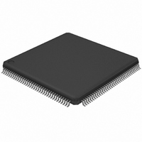
LPC2388FBD144,551 NXP Semiconductors, LPC2388FBD144,551 Datasheet - Page 34

LPC2388FBD144,551
Manufacturer Part Number
LPC2388FBD144,551
Description
IC ARM7 MCU FLASH 512K 144LQFP
Manufacturer
NXP Semiconductors
Series
LPC2300r
Specifications of LPC2388FBD144,551
Program Memory Type
FLASH
Program Memory Size
512KB (512K x 8)
Package / Case
144-LQFP
Core Processor
ARM7
Core Size
16/32-Bit
Speed
72MHz
Connectivity
CAN, EBI/EMI, Ethernet, I²C, Microwire, MMC, SPI, SSI, SSP, UART/USART, USB OTG
Peripherals
Brown-out Detect/Reset, DMA, I²S, POR, PWM, WDT
Number Of I /o
104
Ram Size
98K x 8
Voltage - Supply (vcc/vdd)
3 V ~ 3.6 V
Data Converters
A/D 8x10b; D/A 1x10b
Oscillator Type
Internal
Operating Temperature
-40°C ~ 85°C
Processor Series
LPC23
Core
ARM7TDMI-S
Data Bus Width
16 bit, 32 bit
Data Ram Size
98 KB
Interface Type
CAN/I2C/I2S/SPI/SSP/UART/USB
Maximum Clock Frequency
72 MHz
Number Of Programmable I/os
104
Number Of Timers
4
Operating Supply Voltage
3.3 V
Maximum Operating Temperature
+ 85 C
Mounting Style
SMD/SMT
3rd Party Development Tools
MDK-ARM, RL-ARM, ULINK2, MCB2388, MCB2388U, MCB2388UME
Development Tools By Supplier
OM11012
Minimum Operating Temperature
- 40 C
On-chip Adc
8-ch x 10-bit
On-chip Dac
1-ch x 10-bit
Lead Free Status / RoHS Status
Lead free / RoHS Compliant
For Use With
OM11012 - BOARD EVAL FOR LPC2388568-3999 - BOARD EVAL FOR LPC23 ARM MCU622-1005 - USB IN-CIRCUIT PROG ARM7 LPC2K
Eeprom Size
-
Lead Free Status / Rohs Status
Lead free / RoHS Compliant
Other names
568-4323
935285417551
LPC2388FBD144-S
935285417551
LPC2388FBD144-S
Available stocks
Company
Part Number
Manufacturer
Quantity
Price
Company:
Part Number:
LPC2388FBD144,551
Manufacturer:
NXP Semiconductors
Quantity:
10 000
NXP Semiconductors
LPC2388_0
Preliminary data sheet
7.26.1 Reset
7.26.2 Brownout detection
7.26 System control
The first option assumes that power consumption is not a concern and the design ties the
V
supply for both pads, the CPU, and peripherals. While this solution is simple, it does not
support powering down the I/O pad ring “on the fly” while keeping the CPU and
peripherals alive.
The second option uses two power supplies; a 3.3 V supply for the I/O pads (V
a dedicated 3.3 V supply for the CPU (V
converter powered independently from the I/O pad ring enables shutting down of the I/O
pad power supply “on the fly”, while the CPU and peripherals stay active.
The VBAT pin supplies power only to the RTC and the Battery RAM. These two functions
require a minimum of power to operate, which can be supplied by an external battery.
When the CPU and the rest of chip functions are stopped and power removed, the RTC
can supply an alarm output that may be used by external hardware to restore chip power
and resume operation.
Reset has four sources on the LPC2388: the RESET pin, the Watchdog reset, power-on
reset, and the BrownOut Detection (BOD) circuit. The RESET pin is a Schmitt trigger input
pin. Assertion of chip Reset by any source, once the operating voltage attains a usable
level, starts the Wake-up timer (see description in
causing reset to remain asserted until the external Reset is de-asserted, the oscillator is
running, a fixed number of clocks have passed, and the flash controller has completed its
initialization.
When the internal Reset is removed, the processor begins executing at address 0, which
is initially the Reset vector mapped from the Boot Block. At that point, all of the processor
and peripheral registers have been initialized to predetermined values.
The LPC2388 includes 2-stage monitoring of the voltage on the V
voltage falls below 2.95 V, the BOD asserts an interrupt signal to the Vectored Interrupt
Controller. This signal can be enabled for interrupt in the Interrupt Enable Register in the
VIC in order to cause a CPU interrupt; if not, software can monitor the signal by reading a
dedicated status register.
The second stage of low-voltage detection asserts Reset to inactivate the LPC2388 when
the voltage on the V
flash as operation of the various elements of the chip would otherwise become unreliable
due to low voltage. The BOD circuit maintains this reset down below 1 V, at which point
the power-on reset circuitry maintains the overall Reset.
Both the 2.95 V and 2.65 V thresholds include some hysteresis. In normal operation, this
hysteresis allows the 2.95 V detection to reliably interrupt, or a regularly executed event
loop to sense the condition.
DD(3V3)
and V
DD(DCDC)(3V3)
DD(3V3)
Rev. 00.01 — 23 October 2007
pins falls below 2.65 V. This Reset prevents alteration of the
pins together. This approach requires only one 3.3 V power
DD(DCDC)(3V3)
Section 7.25.3 “Wake-up
). Having the on-chip DC-to-DC
Fast communication chip
DD(3V3)
LPC2388
© NXP B.V. 2007. All rights reserved.
pins. If this
timer”),
DD(3V3)
34 of 57
) and


