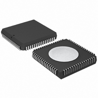
P87C554SBAA,512 NXP Semiconductors, P87C554SBAA,512 Datasheet - Page 6

P87C554SBAA,512
Manufacturer Part Number
P87C554SBAA,512
Description
IC 80C51 MCU 16K OTP 64-PLCC
Manufacturer
NXP Semiconductors
Series
87Cr
Specifications of P87C554SBAA,512
Core Processor
8051
Core Size
8-Bit
Speed
16MHz
Connectivity
EBI/EMI, I²C, UART/USART
Peripherals
POR, PWM, WDT
Number Of I /o
40
Program Memory Size
16KB (16K x 8)
Program Memory Type
OTP
Ram Size
512 x 8
Voltage - Supply (vcc/vdd)
2.7 V ~ 5.5 V
Data Converters
A/D 8x10b
Oscillator Type
Internal
Operating Temperature
0°C ~ 70°C
Package / Case
68-PLCC
Cpu Family
87C
Device Core
80C51
Device Core Size
8b
Frequency (max)
16MHz
Interface Type
I2C/UART
Total Internal Ram Size
512Byte
# I/os (max)
40
Number Of Timers - General Purpose
3
Operating Supply Voltage (typ)
5V
Operating Supply Voltage (max)
5.5V
Operating Supply Voltage (min)
4.5V
On-chip Adc
7-chx10-bit
Instruction Set Architecture
CISC
Operating Temp Range
0C to 70C
Operating Temperature Classification
Commercial
Mounting
Surface Mount
Pin Count
68
Package Type
PLCC
Processor Series
P87C5x
Core
80C51
Data Bus Width
8 bit
Data Ram Size
512 B
Maximum Clock Frequency
16 MHz
Number Of Programmable I/os
40
Number Of Timers
3
Operating Supply Voltage
2.7 V to 5.5 V
Maximum Operating Temperature
+ 70 C
Mounting Style
SMD/SMT
3rd Party Development Tools
PK51, CA51, A51, ULINK2
Minimum Operating Temperature
0 C
Lead Free Status / RoHS Status
Lead free / RoHS Compliant
Eeprom Size
-
Lead Free Status / Rohs Status
Compliant
Other names
568-1254-5
935263385512
P87C554SBAA
935263385512
P87C554SBAA
Available stocks
Company
Part Number
Manufacturer
Quantity
Price
Company:
Part Number:
P87C554SBAA,512
Manufacturer:
NXP Semiconductors
Quantity:
10 000
Philips Semiconductors
PIN DESCRIPTION
Table 1. Pin description
2002 Mar 25
V
STADC
PWM0
PWM1
EW
P0.0-P0.7
P1.0-P1.7
P2.0-P2.7
P3.0-P3.7
DD
80C51 8-bit microcontroller – 12 clock operation
16K/512 OTP/RAM, 8 channel 10-bit A/D, I
capture/compare, high I/O
MNEMONIC
PIN NO.
57-50
16-23
16-21
22-23
16-19
39-46
24-31
20
21
22
23
24
25
26
27
28
29
30
31
2
3
4
5
6
TYPE
I/O
I/O
I/O
I/O
I/O
I/O
I/O
I/O
O
O
I
I
I
I
I
I
Digital Power Supply: Positive voltage power supply pin during normal operation, idle and
power-down mode.
Start ADC Operation: Input starting analog to digital conversion (ADC operation can also be
started by software).
Pulse Width Modulation: Output 0.
Pulse Width Modulation: Output 1.
Enable Watchdog Timer: Enable for T3 watchdog timer and disable power-down mode.
Port 0: Port 0 is an 8-bit open-drain bidirectional I/O port. Port 0 pins that have 1s written to them
float and can be used as high-impedance inputs. Port 0 is also the multiplexed low-order address
and data bus during accesses to external program and data memory. In this application it uses
strong internal pull-ups when emitting 1s. Port 0 is also used to input the code byte during
programming and to output the code byte during verification.
Port 1: 8-bit I/O port. Alternate functions include:
(P1.0-P1.5): Programmable I/O port pins.
(P1.6, P1.7): Open drain port pins.
CT0I-CT3I (P1.0-P1.3): Capture timer input signals for timer T2.
T2 (P1.4): T2 event input.
RT2 (P1.5): T2 timer reset signal. Rising edge triggered.
SCL (P1.6): Serial port clock line I
SDA (P1.7): Serial port data line I
Port 1 has four modes selected on a per bit basis by writing to the P1M1 and P1M2 registers as
follows:
Port 1 is also used to input the lower order address byte during EPROM programming and
verification. A0 is on P1.0, etc.
Port 2: 8-bit programmable I/O port.
Alternate function: High-order address byte for external memory (A08-A15). Port 2 is also used to
input the upper order address during EPROM programming and verification. A8 is on P2.0, A9 on
P2.1, through A13 on P2.5.
Port 2 has four output modes selected on a per bit basis by writing to the P2M1 and P2M2 registers
as follows:
Port 3: 8-bit programmable I/O port. Alternate functions include:
RxD(P3.0): Serial input port.
TxD (P3.1): Serial output port.
INT0 (P3.2): External interrupt.
INT1 (P3.3): External interrupt.
T0 (P3.4): Timer 0 external input.
T1 (P3.5): Timer 1 external input.
WR (P3.6): External data memory write strobe.
RD (P3.7): External data memory read strobe.
Port 3 has four modes selected on a per bit basis by writing to the P3M1 and P3M2 registers as
follows:
P1M1.x
0
0
1
1
P2M1.x
0
0
1
1
P3M1.x
0
0
1
1
P1M2.x
0
1
0
1
P2M2.x
0
1
0
1
P3M2.x
0
1
0
1
2
C, PWM,
4
Mode Description
Pseudo–bidirectional (standard c51 configuration; default)
Push-Pull
High impedance
Open drain
Mode Description
Pseudo–bidirectional (standard c51 configuration; default)
Push-Pull
High impedance
Open drain
Mode Description
Pseudo–bidirectional (standard c51 configuration; default)
Push–Pull
High impedance
Open drain
2
2
C-bus.
C-bus.
NAME AND FUNCTION
P87C554
Product data


