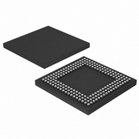
LPC2888FET180/01,5 NXP Semiconductors, LPC2888FET180/01,5 Datasheet - Page 9

LPC2888FET180/01,5
Manufacturer Part Number
LPC2888FET180/01,5
Description
IC ARM7 MCU FLASH 1MB 180TFBGA
Manufacturer
NXP Semiconductors
Series
LPC2800r
Datasheet
1.LPC2888FET180015.pdf
(43 pages)
Specifications of LPC2888FET180/01,5
Core Processor
ARM7
Core Size
16/32-Bit
Speed
60MHz
Connectivity
EBI/EMI, I²C, IrDA, MMC, UART/USART, USB
Peripherals
DMA, I²S, LCD, WDT
Number Of I /o
85
Program Memory Size
1MB (1M x 8)
Program Memory Type
FLASH
Ram Size
64K x 8
Voltage - Supply (vcc/vdd)
1.7 V ~ 3.6 V
Data Converters
A/D 5x10b
Oscillator Type
External
Operating Temperature
-40°C ~ 85°C
Package / Case
180-TFBGA
Processor Series
LPC28
Core
ARM7TDMI-S
Data Bus Width
32 bit
Data Ram Size
64 KB
Interface Type
I2C, I2S, UART, USB
Maximum Clock Frequency
60 MHz
Number Of Programmable I/os
81
Number Of Timers
2
Operating Supply Voltage
1.8 V, 3.3 V
Maximum Operating Temperature
+ 85 C
Mounting Style
SMD/SMT
3rd Party Development Tools
MDK-ARM, RL-ARM, ULINK2
Development Tools By Supplier
OM10092
Minimum Operating Temperature
- 40 C
On-chip Adc
10 bit, 5 Channel
For Use With
OM10092 - EVAL BOARD FOR LPC288X
Lead Free Status / RoHS Status
Lead free / RoHS Compliant
Eeprom Size
-
Lead Free Status / Rohs Status
Details
Other names
568-4528
NXP Semiconductors
Table 4.
LPC2880_LPC2888_3
Preliminary data sheet
Symbol
CKE/P1[9]
DQM0/P1[10]
DQM1/P1[11]
DYCS/P1[8]
MCLKO/P1[14]
OE/P1[18]
RAS/P1[17]
RPO/P1[19]
STCS0/P1[5]
STCS1/P1[6]
STCS2/P1[7]
WE/P1[15]
GPIO and mode control
MODE1/P2[2]
MODE2/P2[3]
P2[0]
P2[1]
I
SCL
SDA
JTAG interface
JTAG_SEL
JTAG_TCK
JTAG_TDI
JTAG_TMS
JTAG_TRST
JTAG_TDO
LCD interface
LCS/P4[0]
LD0/P4[4]
LD1/P4[5]
LD2/P4[6]
LD3/P4[7]
LD4/P4[8]
LD5/P4[9]
LD6/P4[10]
LD7/P4[11]
LER/P4[3]
LRS/P4[1]
LRW/P4[2]
2
C-bus interface
Pin description
Ball #
B10
C12
A11
B9
A10
A17
A9
B1
C9
A8
B11
C11
K18
J16
K16
K17
H16
J17
U4
V4
T5
U12
T13
U13
B3
C2
C1
C3
D2
D1
D3
E2
E3
F2
F3
G2
…continued
Type
FO
FO
FO
FO
FO
FO
FO
FO
FO
FO
FO
FO
FI
FI
FI
FI
I/O
I/O
I
I
I
I
I
O
FO
FO
FO
FO
FO
FO
FO
FO
FO
FO
FO
FO
[1]
Description
clock enable; active HIGH for SDRAM; GPIO pin
data mask output for D[7:0], active HIGH for SDRAM; GPIO pin
data mask output for D[15:8], active HIGH for SDRAM; GPIO pin
chip select, active LOW for SDRAM; GPIO pin
clock for SDRAM and SyncFlash memory; GPIO pin
output enable, active LOW for static memory; GPIO pin
row address strobe, active LOW for SDRAM; GPIO pin
reset power-down, active LOW for SyncFlash memory; GPIO pin
chip select, active LOW for static memory bank 0; GPIO pin
chip select, active LOW for static memory bank 1; GPIO pin
chip select, active LOW for static memory bank 2; GPIO pin
write enable, active LOW for SDRAM and static memory; GPIO pin
start-up mode pin 1 (pull-down); 5 V tolerant GPIO pin
start-up mode pin 2 (pull-down); 5 V tolerant GPIO pin
5 V tolerant GPIO pin
5 V tolerant GPIO pin
serial clock (input/open-drain output); 5 V tolerant pin
serial data (input/open-drain output); 5 V tolerant pin
JTAG selection (pull-down); 5 V tolerant pin
JTAG reset input (pull-down); 5 V tolerant pin
JTAG data input (pull-up); 5 V tolerant pin
JTAG mode select input (pull-up); 5 V tolerant pin
JTAG reset input (pull-down); 5 V tolerant pin
JTAG data output; 5 V tolerant pin
chip select to LCD device, programmable polarity; 5 V tolerant GPIO pin
data bus to/from LCD (I/O) or 5 V tolerant GPIO pins
6800 E or 8080 RD or 5 V tolerant GPIO pin
‘HIGH’ data register select, ‘LOW’ instruction register select, or 5 V tolerant
GPIO pin
6800 W/R or 8080 WR or 5 V tolerant GPIO pin
16/32-bit ARM microcontrollers with external memory interface
Rev. 03 — 17 April 2008
LPC2880; LPC2888
© NXP B.V. 2008. All rights reserved.
9 of 43


