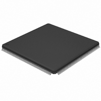
LPC2468FBD208,551 NXP Semiconductors, LPC2468FBD208,551 Datasheet - Page 45

LPC2468FBD208,551
Manufacturer Part Number
LPC2468FBD208,551
Description
IC ARM7 MCU FLASH 512K 208-LQFP
Manufacturer
NXP Semiconductors
Series
LPC2400r
Specifications of LPC2468FBD208,551
Program Memory Type
FLASH
Program Memory Size
512KB (512K x 8)
Package / Case
208-LQFP
Core Processor
ARM7
Core Size
16/32-Bit
Speed
72MHz
Connectivity
CAN, EBI/EMI, Ethernet, I²C, Microwire, MMC, SPI, SSI, SSP, UART/USART, USB OTG
Peripherals
Brown-out Detect/Reset, DMA, I²S, POR, PWM, WDT
Number Of I /o
160
Ram Size
98K x 8
Voltage - Supply (vcc/vdd)
3 V ~ 3.6 V
Data Converters
A/D 8x10b; D/A 1x10b
Oscillator Type
Internal
Operating Temperature
-40°C ~ 85°C
Processor Series
LPC24
Core
ARM7TDMI-S
Data Bus Width
16 bit, 32 bit
Data Ram Size
98 KB
Interface Type
CAN/I2S/ISP/SSP/UART/USB
Maximum Clock Frequency
72 MHz
Number Of Programmable I/os
160
Number Of Timers
6
Operating Supply Voltage
3.3 V
Maximum Operating Temperature
+ 85 C
Mounting Style
SMD/SMT
3rd Party Development Tools
MDK-ARM, RL-ARM, ULINK2, IRD-LPC2468-DEV, SAB-TFBGA208, KSK-LPC2468-PL
Development Tools By Supplier
OM10100
Minimum Operating Temperature
- 40 C
On-chip Adc
8-ch x 10-bit
On-chip Dac
1-ch x 10-bit
Lead Free Status / RoHS Status
Lead free / RoHS Compliant
For Use With
622-1025 - KIT DEV IND REF DESIGN LPC2468622-1024 - BOARD SCKT ADAPTER FOR TFBGA208568-4358 - DISPLAY QVGA TFT FOR OM10100568-4309 - BOARD EXTENSION LPCSTICK568-4308 - EVAL LPC-STICK WITH LPC2468MCB2400U - BOARD EVAL MCB2400 + ULINK2MCB2400 - BOARD EVAL FOR NXP LPC246X SER622-1005 - USB IN-CIRCUIT PROG ARM7 LPC2K
Eeprom Size
-
Lead Free Status / Rohs Status
Lead free / RoHS Compliant
Other names
568-4261
935282457551
LPC2468FBD208-S
935282457551
LPC2468FBD208-S
Available stocks
Company
Part Number
Manufacturer
Quantity
Price
Company:
Part Number:
LPC2468FBD208,551
Manufacturer:
TI
Quantity:
1 908
Company:
Part Number:
LPC2468FBD208,551
Manufacturer:
NXP Semiconductors
Quantity:
10 000
NXP Semiconductors
LPC2468
Product data sheet
CAUTION
7.26.4 AHB
7.26.5 External interrupt inputs
7.26.6 Memory mapping control
7.27.1 EmbeddedICE
7.27 Emulation and debugging
The LPC2468 implements two AHB in order to allow the Ethernet block to operate without
interference caused by other system activity. The primary AHB, referred to as AHB1,
includes the Vectored Interrupt Controller, GPDMA controller, USB interface, and 16 kB
SRAM.
The second AHB, referred to as AHB2, includes only the Ethernet block and an
associated 16 kB SRAM. In addition, a bus bridge is provided that allows the secondary
AHB to be a bus master on AHB1, allowing expansion of Ethernet buffer space into
off-chip memory or unused space in memory residing on AHB1.
In summary, bus masters with access to AHB1 are the ARM7 itself, the USB block, the
GPDMA function, and the Ethernet block (via the bus bridge from AHB2). Bus masters
with access to AHB2 are the ARM7 and the Ethernet block.
The LPC2468 includes up to 68 edge sensitive interrupt inputs combined with up to four
level sensitive external interrupt inputs as selectable pin functions. The external interrupt
inputs can optionally be used to wake up the processor from Power-down mode.
The memory mapping control alters the mapping of the interrupt vectors that appear at the
beginning at address 0x0000 0000. Vectors may be mapped to the bottom of the Boot
ROM, the SRAM, or external memory. This allows code running in different memory
spaces to have control of the interrupts.
The LPC2468 support emulation and debugging via a JTAG serial port. A trace port allows
tracing program execution. Debugging and trace functions are multiplexed only with
GPIOs on P2[0] to P2[9]. This means that all communication, timer, and interface
peripherals residing on other pins are available during the development and debugging
phase as they are when the application is run in the embedded system itself.
The EmbeddedICE logic provides on-chip debug support. The debugging of the target
system requires a host computer running the debugger software and an EmbeddedICE
protocol convertor. The EmbeddedICE protocol convertor converts the Remote Debug
Protocol commands to the JTAG data needed to access the ARM7TDMI-S core present
on the target system.
The ARM core has a Debug Communication Channel (DCC) function built-in. The DCC
allows a program running on the target to communicate with the host debugger or another
separate host without stopping the program flow or even entering the debug state. The
If level three Code Read Protection (CRP3) is selected, no future factory testing can be
performed on the device.
All information provided in this document is subject to legal disclaimers.
Rev. 5 — 15 October 2010
Single-chip 16-bit/32-bit micro
LPC2468
© NXP B.V. 2010. All rights reserved.
45 of 85


