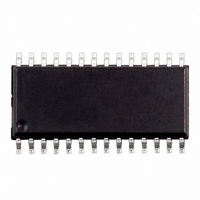
ST72F262G1M6 STMicroelectronics, ST72F262G1M6 Datasheet - Page 113

ST72F262G1M6
Manufacturer Part Number
ST72F262G1M6
Description
MCU 8BIT 4KB FLASH 28-SOIC
Manufacturer
STMicroelectronics
Series
ST7r
Datasheet
1.STEVAL-ISQ002V1.pdf
(172 pages)
Specifications of ST72F262G1M6
Core Processor
ST7
Core Size
8-Bit
Speed
16MHz
Connectivity
SPI
Peripherals
LVD, POR, PWM, WDT
Number Of I /o
22
Program Memory Size
4KB (4K x 8)
Program Memory Type
FLASH
Ram Size
256 x 8
Voltage - Supply (vcc/vdd)
2.7 V ~ 5.5 V
Data Converters
A/D 6x10b
Oscillator Type
Internal
Operating Temperature
-40°C ~ 85°C
Package / Case
28-SOIC (7.5mm Width)
Controller Family/series
ST7
No. Of I/o's
22
Ram Memory Size
256Byte
Cpu Speed
8MHz
No. Of Timers
2
Embedded Interface Type
I2C, SCI, SPI
Rohs Compliant
Yes
Processor Series
ST72F2x
Core
ST7
Data Bus Width
8 bit
Data Ram Size
256 B
Interface Type
I2C, SCI, SPI
Maximum Clock Frequency
8 MHz
Number Of Programmable I/os
22
Number Of Timers
4 bit
Operating Supply Voltage
2.7 V to 5.5 V
Maximum Operating Temperature
+ 85 C
Mounting Style
SMD/SMT
Development Tools By Supplier
ST7F264-IND/USB, ST72F34X-SK/RAIS, ST7MDT10-DVP3, ST7MDT10-EMU3, STX-RLINK
Minimum Operating Temperature
- 40 C
On-chip Adc
16 bit
For Use With
497-5046 - KIT TOOL FOR ST7/UPSD/STR7 MCU
Lead Free Status / RoHS Status
Lead free / RoHS Compliant
Eeprom Size
-
Lead Free Status / Rohs Status
In Transition
Other names
497-5581-5
Available stocks
Company
Part Number
Manufacturer
Quantity
Price
I
I
Read / Write
Reset Value: 0000 0000 (00h)
Bit 7 = FM/SM Fast/Standard I
This bit is set and cleared by software. It is not
cleared when the interface is disabled (PE=0).
0: Standard I
1: Fast I
Bit 6:0 = CC[6:0] 7-bit clock divider.
These bits select the speed of the bus (F
pending on the I
when the interface is disabled (PE=0).
Refer to the Electrical Characteristics section for
the table of values.
Note: The programmed F
SCL and SDA lines.
FM/SM
2
2
C BUS INTERFACE (Cont’d)
C CLOCK CONTROL REGISTER (CCR)
7
CC6
2
C mode
2
CC5
C mode
2
C mode. They are not cleared
CC4
SCL
CC3
assumes no load on
2
C mode.
CC2
CC1
SCL
CC0
) de-
0
I
Read / Write
Reset Value: 0000 0000 (00h)
Bit 7:0 = D[7:0] 8-bit Data Register.
These bits contain the byte to be received or trans-
mitted on the bus.
– Transmitter mode: Byte transmission start auto-
– Receiver mode: the first data byte is received au-
2
C DATA REGISTER (DR)
matically when the software writes in the DR reg-
ister.
tomatically in the DR register using the least sig-
nificant bit of the address.
Then, the following data bytes are received one
by one after reading the DR register.
D7
7
ST72260Gx, ST72262Gx, ST72264Gx
D6
D5
D4
D3
D2
D1
113/172
D0
0


