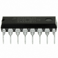
MC9S08QG8CPBE Freescale Semiconductor, MC9S08QG8CPBE Datasheet - Page 58
MC9S08QG8CPBE
Manufacturer Part Number
MC9S08QG8CPBE
Description
IC MCU 8K FLASH 10MHZ 16-DIP
Manufacturer
Freescale Semiconductor
Series
HCS08r
Datasheet
1.MC9S08QG8CDTER.pdf
(314 pages)
Specifications of MC9S08QG8CPBE
Core Processor
HCS08
Core Size
8-Bit
Speed
20MHz
Connectivity
I²C, SCI, SPI
Peripherals
LVD, POR, PWM, WDT
Number Of I /o
12
Program Memory Size
8KB (8K x 8)
Program Memory Type
FLASH
Ram Size
512 x 8
Voltage - Supply (vcc/vdd)
1.8 V ~ 3.6 V
Data Converters
A/D 8x10b
Oscillator Type
Internal
Operating Temperature
-40°C ~ 85°C
Package / Case
16-DIP (0.300", 7.62mm)
Processor Series
S08QG
Core
HCS08
Data Bus Width
8 bit
Data Ram Size
512 B
Interface Type
SCI/SPI
Maximum Clock Frequency
20 MHz
Number Of Programmable I/os
12
Number Of Timers
1
Operating Supply Voltage
1.8 V to 3.6 V
Maximum Operating Temperature
+ 85 C
Mounting Style
Through Hole
3rd Party Development Tools
EWS08
Development Tools By Supplier
DEMO9S08QG8E
Minimum Operating Temperature
- 40 C
On-chip Adc
8-ch x 10-bit
For Use With
DEMO9S08QG8E - BOARD DEMO FOR MC9S08QG8
Lead Free Status / RoHS Status
Lead free / RoHS Compliant
Eeprom Size
-
Lead Free Status / Rohs Status
Lead free / RoHS Compliant
Available stocks
Company
Part Number
Manufacturer
Quantity
Price
Company:

Part Number:
MC9S08QG8CPBE
Manufacturer:
CYPRESS
Quantity:
310


1
Chapter 4 Memory Map and Register Definition
4.7.3
4.7.4
During reset, the contents of the nonvolatile location NVPROT are copied from FLASH into FPROT. This
register can be read at any time. If FPDIS = 0, protection can be increased, i.e., a smaller value of FPS can
be written. If FPDIS = 1, writes do not change protection.
56
Background commands can be used to change the contents of these bits in FPROT.
KEYACC
Reset
Reset
Field
5
W
W
R
R
FLASH Configuration Register (FCNFG)
FLASH Protection Register (FPROT and NVPROT)
Enable Writing of Access Key — This bit enables writing of the backdoor comparison key. For more detailed
information about the backdoor key mechanism, refer to
0 Writes to 0xFFB0–0xFFB7 are interpreted as the start of a FLASH programming or erase command.
1 Writes to NVBACKKEY (0xFFB0–0xFFB7) are interpreted as comparison key writes.
0
0
7
7
= Unimplemented or Reserved
0
0
6
6
Figure 4-7. FLASH Configuration Register (FCNFG)
1
This register is loaded from nonvolatile location NVPROT during reset.
Figure 4-8. FLASH Protection Register (FPROT)
Table 4-10. FCNFG Register Field Descriptions
SEC01:SEC00 changes to 1:0 after successful backdoor
key entry or a successful blank check of FLASH.
MC9S08QG8 and MC9S08QG4 Data Sheet, Rev. 5
SEC01:SEC00
KEYACC
0
5
5
0:0
0:1
1:0
1:1
Table 4-9. Security States
FPS
0
0
4
4
(1)
Description
Section 4.6,
Description
unsecured
secure
secure
secure
3
0
0
3
1
“Security.”
0
0
2
2
Freescale Semiconductor
0
0
1
1
FPDIS
0
0
0
0
(1)
Related parts for MC9S08QG8CPBE
Image
Part Number
Description
Manufacturer
Datasheet
Request
R

Part Number:
Description:
Manufacturer:
Freescale Semiconductor, Inc
Datasheet:
Part Number:
Description:
Manufacturer:
Freescale Semiconductor, Inc
Datasheet:
Part Number:
Description:
Manufacturer:
Freescale Semiconductor, Inc
Datasheet:
Part Number:
Description:
Manufacturer:
Freescale Semiconductor, Inc
Datasheet:
Part Number:
Description:
Manufacturer:
Freescale Semiconductor, Inc
Datasheet:
Part Number:
Description:
Manufacturer:
Freescale Semiconductor, Inc
Datasheet:
Part Number:
Description:
Manufacturer:
Freescale Semiconductor, Inc
Datasheet:
Part Number:
Description:
Manufacturer:
Freescale Semiconductor, Inc
Datasheet:
Part Number:
Description:
Manufacturer:
Freescale Semiconductor, Inc
Datasheet:
Part Number:
Description:
Manufacturer:
Freescale Semiconductor, Inc
Datasheet:
Part Number:
Description:
Manufacturer:
Freescale Semiconductor, Inc
Datasheet:
Part Number:
Description:
Manufacturer:
Freescale Semiconductor, Inc
Datasheet:
Part Number:
Description:
Manufacturer:
Freescale Semiconductor, Inc
Datasheet:
Part Number:
Description:
Manufacturer:
Freescale Semiconductor, Inc
Datasheet:
Part Number:
Description:
Manufacturer:
Freescale Semiconductor, Inc
Datasheet: