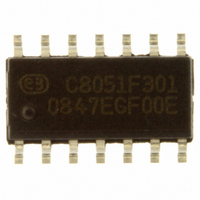
C8051F301-GS Silicon Laboratories Inc, C8051F301-GS Datasheet - Page 157

C8051F301-GS
Manufacturer Part Number
C8051F301-GS
Description
IC 8051 MCU 8K FLASH 14-SOIC
Manufacturer
Silicon Laboratories Inc
Series
C8051F30xr
Specifications of C8051F301-GS
Program Memory Type
FLASH
Program Memory Size
8KB (8K x 8)
Package / Case
14-SOIC (3.9mm Width), 14-SOL
Core Processor
8051
Core Size
8-Bit
Speed
25MHz
Connectivity
SMBus (2-Wire/I²C), UART/USART
Peripherals
POR, PWM, WDT
Number Of I /o
8
Ram Size
256 x 8
Voltage - Supply (vcc/vdd)
2.7 V ~ 3.6 V
Oscillator Type
Internal
Operating Temperature
-40°C ~ 85°C
Processor Series
C8051F3x
Core
8051
Data Bus Width
8 bit
Data Ram Size
256 B
Interface Type
I2C/SMBus/UART
Maximum Clock Frequency
25 MHz
Number Of Programmable I/os
8
Number Of Timers
3
Maximum Operating Temperature
+ 85 C
Mounting Style
SMD/SMT
3rd Party Development Tools
PK51, CA51, A51, ULINK2
Development Tools By Supplier
C8051F300DK
Minimum Operating Temperature
- 40 C
Package
14SOIC
Device Core
8051
Family Name
C8051F30x
Maximum Speed
25 MHz
Operating Supply Voltage
3.3 V
Lead Free Status / RoHS Status
Lead free / RoHS Compliant
For Use With
770-1006 - ISP 4PORT FOR SILABS C8051F MCU336-1444 - ADAPTER PROGRAM TOOLSTICK F300336-1319 - REFERENCE DESIGN STEPPER MOTOR
Eeprom Size
-
Data Converters
-
Lead Free Status / Rohs Status
Lead free / RoHS Compliant
Other names
336-1536-5
16.2. Capture/Compare Modules
Each module can be configured to operate independently in one of six operation modes: Edge-triggered
Capture, Software Timer, High Speed Output, Frequency Output, 8-bit Pulse Width Modulator, or 16-bit
Pulse Width Modulator. Each module has Special Function Registers (SFRs) associated with it in the CIP-
51 system controller. These registers are used to exchange data with a module and configure the module's
mode of operation.
Table 16.2 summarizes the bit settings in the PCA0CPMn registers used to select the PCA capture/com-
pare module’s operating modes. Setting the ECCFn bit in a PCA0CPMn register enables the module's
CCFn interrupt. Note: PCA0 interrupts must be globally enabled before individual CCFn interrupts are rec-
ognized. PCA0 interrupts are globally enabled by setting the EA bit and the EPCA0 bit to logic 1. See
Figure 16.3 for details on the PCA interrupt configuration.
*Note: X = Don’t Care
PWM16 ECOM CAPP CAPN
Timer Overflow
Table 16.2. PCA0CPM Register Settings for PCA Capture/Compare Modules
X*
X*
X*
X*
X*
X*
0
1
PCA Counter/
W
M
P
1
6
n
PCA Module 0
PCA Module 1
PCA Module 2
(for n = 0 to 2)
PCA0CPMn
E
C
O
M
n
C
A
P
P
n
(CCF0)
(CCF1)
(CCF2)
C
N
A
P
n
X*
X*
X*
1
1
1
1
1
M
A
T
n
O
G
T
n
W
M
P
n
E
C
C
F
n
C
F
1
0
1
0
0
0
0
0
C
R
PCA0CN
Figure 16.3. PCA Interrupt Block Diagram
C
C
F
2
0
1
1
0
0
0
0
0
C
C
F
1
C
C
F
0
ECCF0
ECCF1
ECCF2
C
D
L
I
MAT
W
D
T
E
PCA0MD
X*
X*
X*
W
D
C
K
0
0
0
1
1
L
C
P
S
2
C
P
S
1
0
1
0
1
0
1
C
P
S
0
TOG
E
C
F
0
0
0
0
1
1
0
0
Rev. 2.9
0
1
PWM ECCF
0
0
0
0
0
1
1
1
C8051F300/1/2/3/4/5
X*
X*
X*
X*
X*
X*
X*
X*
Capture triggered by positive edge
on CEXn
Capture triggered by negative
edge on CEXn
Capture triggered by transition on
CEXn
Software Timer
High Speed Output
Frequency Output
8-bit Pulse Width Modulator
16-bit Pulse Width Modulator
EPCA0
Operation Mode
0
1
EA
0
1
Interrupt
Priority
Decoder
157


