C8051F301-GS Silicon Laboratories Inc, C8051F301-GS Datasheet - Page 86
C8051F301-GS
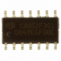
Manufacturer Part Number
C8051F301-GS
Description
IC 8051 MCU 8K FLASH 14-SOIC
Manufacturer
Silicon Laboratories Inc
Series
C8051F30xr
Specifications of C8051F301-GS
Program Memory Type
FLASH
Program Memory Size
8KB (8K x 8)
Package / Case
14-SOIC (3.9mm Width), 14-SOL
Core Processor
8051
Core Size
8-Bit
Speed
25MHz
Connectivity
SMBus (2-Wire/I²C), UART/USART
Peripherals
POR, PWM, WDT
Number Of I /o
8
Ram Size
256 x 8
Voltage - Supply (vcc/vdd)
2.7 V ~ 3.6 V
Oscillator Type
Internal
Operating Temperature
-40°C ~ 85°C
Processor Series
C8051F3x
Core
8051
Data Bus Width
8 bit
Data Ram Size
256 B
Interface Type
I2C/SMBus/UART
Maximum Clock Frequency
25 MHz
Number Of Programmable I/os
8
Number Of Timers
3
Maximum Operating Temperature
+ 85 C
Mounting Style
SMD/SMT
3rd Party Development Tools
PK51, CA51, A51, ULINK2
Development Tools By Supplier
C8051F300DK
Minimum Operating Temperature
- 40 C
Package
14SOIC
Device Core
8051
Family Name
C8051F30x
Maximum Speed
25 MHz
Operating Supply Voltage
3.3 V
Lead Free Status / RoHS Status
Lead free / RoHS Compliant
For Use With
770-1006 - ISP 4PORT FOR SILABS C8051F MCU336-1444 - ADAPTER PROGRAM TOOLSTICK F300336-1319 - REFERENCE DESIGN STEPPER MOTOR
Eeprom Size
-
Data Converters
-
Lead Free Status / Rohs Status
Lead free / RoHS Compliant
Other names
336-1536-5


C8051F300/1/2/3/4/5
9.7.
If a Flash read/write/erase or program read targets an illegal address, a system reset is generated. This
may occur due to any of the following:
•
•
•
The FERROR bit (RSTSRC.6) is set following a Flash error reset. The state of the RST pin is unaffected by
this reset.
9.8.
Software may force a reset by writing a ‘1’ to the SWRSF bit (RSTSRC.4). The SWRSF bit will read ‘1’ fol-
lowing a software forced reset. The state of the RST pin is unaffected by this reset.
Table 9.2. Reset Electrical Characteristics
–40 to +85 °C unless otherwise specified.
86
Missing Clock Detector Timeout Time from last system clock ris-
V
RST Input Leakage Current
DD
Minimum RST Low Time to
Generate a System Reset
A Flash write or erase is attempted above user code space. This occurs when PSWE is set to ‘1’ and a
MOVX operation is attempted above the user code space address limit.
A Flash read is attempted above user code space. This occurs when a MOVC operation is attempted
above the user code space address limit.
A Program read is attempted above user code space. This occurs when user code attempts to branch
to an address above the user code space address limit.
RST Output Low Voltage
RST Input High Voltage
RST Input Low Voltage
Monitor Threshold (V
Reset Time Delay
Flash Error Reset
Software Reset
V
DD
Parameter
Ramp Time
C8051F300/1/2/3
Table 9.1. User Code Space Address Limits
C8051F304
C8051F305
RST
Device
)
reset source and code execution
Delay between release of any
I
OL
ing edge to reset initiation
= 8.5 mA, V
at location 0x0000
V
DD
RST = 0.0 V
Conditions
User Code Space Address Limit
= 0 to V
3.6 V
Rev. 2.9
DD
= 2.7 V to
RST
0x1DFF
0x0FFF
0x07FF
0.7 x V
2.40
Min
100
5.0
15
—
—
—
—
DD
2.55
Typ
220
25
—
—
—
—
—
—
0.3 x V
Max
2.70
500
0.6
40
—
—
—
1
DD
Units
ms
µA
µs
µs
µs
V
V
V
Related parts for C8051F301-GS
Image
Part Number
Description
Manufacturer
Datasheet
Request
R

Part Number:
Description:
SMD/C°/SINGLE-ENDED OUTPUT SILICON OSCILLATOR
Manufacturer:
Silicon Laboratories Inc
Part Number:
Description:
Manufacturer:
Silicon Laboratories Inc
Datasheet:
Part Number:
Description:
N/A N/A/SI4010 AES KEYFOB DEMO WITH LCD RX
Manufacturer:
Silicon Laboratories Inc
Datasheet:
Part Number:
Description:
N/A N/A/SI4010 SIMPLIFIED KEY FOB DEMO WITH LED RX
Manufacturer:
Silicon Laboratories Inc
Datasheet:
Part Number:
Description:
N/A/-40 TO 85 OC/EZLINK MODULE; F930/4432 HIGH BAND (REV E/B1)
Manufacturer:
Silicon Laboratories Inc
Part Number:
Description:
EZLink Module; F930/4432 Low Band (rev e/B1)
Manufacturer:
Silicon Laboratories Inc
Part Number:
Description:
I°/4460 10 DBM RADIO TEST CARD 434 MHZ
Manufacturer:
Silicon Laboratories Inc
Part Number:
Description:
I°/4461 14 DBM RADIO TEST CARD 868 MHZ
Manufacturer:
Silicon Laboratories Inc
Part Number:
Description:
I°/4463 20 DBM RFSWITCH RADIO TEST CARD 460 MHZ
Manufacturer:
Silicon Laboratories Inc
Part Number:
Description:
I°/4463 20 DBM RADIO TEST CARD 868 MHZ
Manufacturer:
Silicon Laboratories Inc
Part Number:
Description:
I°/4463 27 DBM RADIO TEST CARD 868 MHZ
Manufacturer:
Silicon Laboratories Inc
Part Number:
Description:
I°/4463 SKYWORKS 30 DBM RADIO TEST CARD 915 MHZ
Manufacturer:
Silicon Laboratories Inc
Part Number:
Description:
N/A N/A/-40 TO 85 OC/4463 RFMD 30 DBM RADIO TEST CARD 915 MHZ
Manufacturer:
Silicon Laboratories Inc
Part Number:
Description:
I°/4463 20 DBM RADIO TEST CARD 169 MHZ
Manufacturer:
Silicon Laboratories Inc