C8051F300-GM Silicon Laboratories Inc, C8051F300-GM Datasheet
C8051F300-GM
Specifications of C8051F300-GM
Available stocks


Related parts for C8051F300-GM

C8051F300-GM Summary of contents
Page 1
... Quad Flat No-Lead (QFN) Package (Lead-free package available) - 3x3 mm PWB footprint ANALOG DIGITAL I/O PERIPHERALS 10-bit SMBus 200ksps PGA ADC Timer 0 C8051F300/2 only TEMP Timer 1 SENSOR Timer 2 VOLTAGE COMPARATOR PROGRAMMABLE PRECISION INTERNAL OSCILLATOR HIGH-SPEED CONTROLLER CORE 8051 CPU ISP Flash (25MIPS) 12 ...
Page 2
... C8051F300/1/2/3/4/5 2 Rev. 2.6 ...
Page 3
... N : OTES C8051F300/1/2/3/4/5 Rev. 2.6 3 ...
Page 4
... C8051F300/1/2/3/4/5 4 Rev. 2.6 ...
Page 5
... On-Chip Memory............................................................................................... 20 1.3. On-Chip Debug Circuitry................................................................................... 21 1.4. Programmable Digital I/O and Crossbar ........................................................... 21 1.5. Serial Ports ....................................................................................................... 22 1.6. Programmable Counter Array ........................................................................... 23 1.7. 8-Bit Analog to Digital Converter (C8051F300/2 Only) ..................................... 24 1.8. Comparator ....................................................................................................... 25 2. Absolute Maximum Ratings .................................................................................. 26 3. Global DC Electrical Characteristics .................................................................... 27 4. Pinout and Package Definitions............................................................................ 28 5 ...
Page 6
... C8051F300/1/2/3/4/5 8.3.4. Interrupt Latency ...................................................................................... 71 8.3.5. Interrupt Register Descriptions................................................................. 73 8.4. Power Management Modes .............................................................................. 78 8.4.1. Idle Mode.................................................................................................. 78 8.4.2. Stop Mode ................................................................................................ 79 9. Reset Sources......................................................................................................... 81 9.1. Power-On Reset ............................................................................................... 82 9.2. Power-Fail Reset / VDD Monitor....................................................................... 82 9.3. External Reset .................................................................................................. 83 9.4. Missing Clock Detector Reset........................................................................... 83 9.5. Comparator0 Reset........................................................................................... 83 9.6. PCA Watchdog Timer Reset............................................................................. 83 9 ...
Page 7
... Pulse Width Modulator Mode......................................................... 158 16.2.6.16-Bit Pulse Width Modulator Mode....................................................... 159 16.3.Watchdog Timer Mode ................................................................................... 160 16.3.1.Watchdog Timer Operation .................................................................... 160 16.3.2.Watchdog Timer Usage ......................................................................... 161 16.4.Register Descriptions for PCA........................................................................ 163 17. C2 Interface ........................................................................................................... 169 17.1.C2 Interface Registers.................................................................................... 169 17.2.C2 Pin Sharing ............................................................................................... 171 C8051F300/1/2/3/4/5 Rev. 2.6 7 ...
Page 8
... C8051F300/1/2/3/4 OTES 8 Rev. 2.6 ...
Page 9
... Table 2.1. Absolute Maximum Ratings* .................................................................. 26 3. Global DC Electrical Characteristics Table 3.1. Global DC Electrical Characteristics ....................................................... 27 4. Pinout and Package Definitions Table 4.1. Pin Definitions for the C8051F300/1/2/3/4/5 ........................................... 28 Table 4.2. QFN-11 Package Diminsions ................................................................. 30 5. ADC0 (8-Bit ADC, C8051F300/2) Table 5.1. ADC0 Electrical Characteristics .............................................................. 45 6 ...
Page 10
... C8051F300/1/2/3/4/5 Table 14.4. Timer Settings for Standard Baud Rates Using an External 18.432 MHz Oscillator ............................................................................................. 136 Table 14.5. Timer Settings for Standard Baud Rates Using an External 11.0592 MHz Oscillator ............................................................................................. 137 Table 14.6. Timer Settings for Standard Baud Rates Using an External 3.6864 MHZ Oscillator ...
Page 11
... Figure 1.1. C8051F300/2 Block Diagram ................................................................. 17 Figure 1.2. C8051F301/3/4/5 Block Diagram ........................................................... 17 Figure 1.3. Comparison of Peak MCU Execution Speeds ....................................... 18 Figure 1.4. On-Chip Clock and Reset ...................................................................... 19 Figure 1.5. On-chip Memory Map (C8051F300/1/2/3 Shown) ................................. 20 Figure 1.6. Development/In-System Debug Diagram............................................... 21 Figure 1.7. Digital Crossbar Diagram ....................................................................... 22 Figure 1.8. PCA Block Diagram ............................................................................... 23 Figure 1 ...
Page 12
... C8051F300/1/2/3/4/5 Figure 11.2. 32.768 kHz External Crystal Example.................................................. 97 12. Port Input/Output Figure 12.1. Port I/O Functional Block Diagram ....................................................... 99 Figure 12.2. Port I/O Cell Block Diagram ................................................................. 99 Figure 12.3. Crossbar Priority Decoder with XBR0 = 0x00 .................................... 100 Figure 12.4. Crossbar Priority Decoder with XBR0 = 0x44 .................................... 101 13 ...
Page 13
... List of Registers SFR Definition 5.1. AMX0SL: AMUX0 Channel Select (C8051F300/ SFR Definition 5.2. ADC0CF: ADC0 Configuration (C8051F300/ SFR Definition 5.3. ADC0: ADC0 Data Word (C8051F300/ SFR Definition 5.4. ADC0CN: ADC0 Control (C8051F300/ SFR Definition 5.5. ADC0GT: ADC0 Greater-Than Data Byte (C8051F300/ SFR Definition 5 ...
Page 14
... C8051F300/1/2/3/4/5 SFR Definition 15.4. TL0: Timer 0 Low Byte . . . . . . . . . . . . . . . . . . . . . . . . . . . . . . . . 146 SFR Definition 15.5. TL1: Timer 1 Low Byte . . . . . . . . . . . . . . . . . . . . . . . . . . . . . . . . 146 SFR Definition 15.6. TH0: Timer 0 High Byte . . . . . . . . . . . . . . . . . . . . . . . . . . . . . . . 146 SFR Definition 15.7. TH1: Timer 1 High Byte . . . . . . . . . . . . . . . . . . . . . . . . . . . . . . . 146 SFR Definition 15.8. TMR2CN: Timer 2 Control . . . . . . . . . . . . . . . . . . . . . . . . . . . . . 149 SFR Definition 15.9. TMR2RLL: Timer 2 Reload Register Low Byte . . . . . . . . . . . . . 150 SFR Definition 15 ...
Page 15
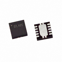
... Each device is specified for 2.7 to 3.6 V operation over the industrial temperature range (–45 to +85 °C). The Port I/O and /RST pins are tolerant of input signals The C8051F300/1/2/3/4/5 are available in the 11-pin QFN package (also referred to as MLP or MLF package) shown in Figure 4.2. ...
Page 16
... C8051F300/1/2/3/4/5 Table 1.1. Product Selection Guide C8051F300 C8051F300- C8051F301 C8051F301- C8051F302 C8051F302- C8051F303 C8051F303- C8051F304 C8051F304- C8051F305 C8051F305- 256 3 8 256 3 8 256 3 8 256 3 8 256 — 256 — 256 — 256 — 256 — 256 — 256 — 256 — ...
Page 17
... GND C2D Debug HW Reset /RST/C2CK Brown- POR Out External XTAL1 Oscillator XTAL2 Circuit System Clock Precision Internal Oscillator Figure 1.1. C8051F300/2 Block Diagram Analog/Digital VDD Power GND C2D Debug HW Reset /RST/C2CK Brown- POR Out External XTAL1 Oscillator XTAL2 Circuit System Clock ...
Page 18
... CIP-51™ Microcontroller Core 1.1.1. Fully 8051 Compatible The C8051F300/1/2/3/4/5 family utilizes Silicon Labs' proprietary CIP-51 microcontroller core. The CIP-51 is fully compatible with the MCS-51™ instruction set; standard 803x/805x assemblers and compilers can be used to develop software. The CIP-51 core offers all the peripherals included with a standard 8052, ...
Page 19
... The WDT may be permanently enabled in software after a power- on reset during MCU initialization. The internal oscillator is available as a factory calibrated 24.5 MHz ±2% (C8051F300/1 devices); an uncal- ibrated version is available on C8051F302/3/4/5 devices. On all C8051F300/1/2/3/4/5 devices, the internal oscillator period may be user programmed in ~0.5% increments. An external oscillator drive circuit is also included, allowing an external crystal, ceramic resonator, capacitor, RC, or CMOS clock source to generate the system clock ...
Page 20
... RAM are accessible via direct and indirect addressing. The first 32 bytes are addressable as four banks of general purpose registers, and the next 16 bytes can be byte addressable or bit addressable. The C8051F300/1/2/3 includes 8k bytes of Flash program memory (the C8051F304 includes 4k bytes; the C8051F305 includes 2k bytes). This memory may be reprogrammed in-system in 512 byte sectors, and requires no special off-chip programming voltage ...
Page 21
... Programmable Digital I/O and Crossbar C8051F300/1/2/3/4/5 devices include a byte-wide I/O Port that behaves like a typical 8051 Port with a few enhancements. Each Port pin may be configured as an analog input or a digital I/O pin. Pins selected as digital I/Os may additionally be configured for push-pull or open-drain output. The “weak pull-ups” that are fixed on typical 8051 devices may be globally disabled, providing power savings capabilities ...
Page 22
... Figure 1.7. Digital Crossbar Diagram 1.5. Serial Ports The C8051F300/1/2/3/4/5 Family includes an SMBus/I2C interface and a full-duplex UART with enhanced baud rate configuration. Each of the serial buses is fully implemented in hardware and makes extensive use of the CIP-51's interrupts, thus requiring very little CPU intervention. ...
Page 23
... WDT mode. The PCA Capture/Compare Module I/O and External Clock Input may be routed to Port I/O via the Digital Crossbar. SYSCLK/12 SYSCLK/4 Timer 0 Overflow ECI SYSCLK External Clock/8 Capture/Compare Module 0 Figure 1.9. PCA Block Diagram C8051F300/1/2/3/4/5 PCA 16-Bit Counter/Timer CLOCK MUX Capture/Compare Module 1 Digital Crossbar Port I/O Rev. 2.6 Capture/Compare ...
Page 24
... Analog to Digital Converter (C8051F300/2 Only) The C8051F300/2 includes an on-chip 8-bit SAR ADC with a 10-channel differential input multiplexer and programmable gain amplifier. With a maximum throughput of 500 ksps, the ADC offers true 8-bit accuracy with an INL of ±1LSB. The ADC system includes a configurable analog multiplexer that selects both posi- tive and negative ADC inputs. Each Port pin is available as an ADC input ...
Page 25
... Comparator C8051F300/1/2/3/4/5 devices include an on-chip voltage comparator that is enabled/disabled and config- ured via user software. All Port I/O pins may be configurated as comparator inputs. Two comparator out- puts may be routed to a Port pin if desired: a latched output and/or an unlatched (asynchronous) output. Comparator response time is programmable, allowing the user to select between high-speed and low- power modes ...
Page 26
... C8051F300/1/2/3/4/5 2. Absolute Maximum Ratings Table 2.1. Absolute Maximum Ratings* Parameter Ambient temperature under bias Storage Temperature Voltage on any Port I/O Pin or /RST with respect to GND Voltage on V with respect to GND DD Maximum Total current through V DD Maximum output current sunk by /RST or any Port pin *Note: Stresses above those listed under “ ...
Page 27
... Digital Supply Current (shutdown) Digital Supply RAM Data Reten- tion Voltage Specified Operating Temperature Range SYSCLK (system clock frequency) Tsysl (SYSCLK low time) Tsysh (SYSCLK high time) *Note: SYSCLK must be at least 32 kHz to enable debugging. C8051F300/1/2/3/4/5 Conditions Min 2 2.7 V, Clock = 25 MHz 2.7 V, Clock = 1 MHz ...
Page 28
... C8051F300/1/2/3/4/5 4. Pinout and Package Definitions Table 4.1. Pin Definitions for the C8051F300/1/2/3/4/5 Pin Number Name 1 VREF / P0 XTAL1 / P0.2 5 XTAL2 / P0.3 6 P0.4 7 P0.5 8 C2CK / /RST 9 P0.6 / CNVSTR 10 C2D / P0.7 11 GND 28 Type Description A In External Voltage Reference Input. D I/O or Port 0.0. See ...
Page 29
... VREF / P0.0 P0.1 VDD XTAL1 / P0.2 XTAL2 / P0.3 Figure 4.1. QFN-11 Pinout Diagram (Top View) C8051F300/1/2/3/4/5 GND Rev. 2.6 C2D / P0.7 P0.6 / CNVSTR C2CK / /RST P0.5 P0.4 29 ...
Page 30
... C8051F300/1/2/3/4/5 Bottom View Side E View e Side D View e Figure 4.2. QFN-11 Package Drawing 30 Table 4.2. QFN-11 Package Diminsions E3 MIN 0.09 Rev. 2.6 MM TYP MAX 0.90 1.00 0.02 0.05 0.65 1.00 0.25 0.23 0.30 3.00 2.20 2.25 2.00 0.386 3.00 1.36 1 ...
Page 31
... L k Figure 4.3. Typical QFN-11 Solder Paste Mask C8051F300/1/2/3/4 0.50 mm 0.35 mm 0. 0.60 mm 0. Rev. 2.6 0. ...
Page 32
... C8051F300/1/2/3/4/5 . 0.10 mm 0.35 mm 0.50 mm 0. Figure 4.4. Typical QFN-11 Landing Diagram 0. Rev. 2.6 ...
Page 33
... ADC0 (8-Bit ADC, C8051F300/2) The ADC0 subsystem for the C8051F300/2 consists of two analog multiplexers (referred to collectively as AMUX0) with 11 total input selections, a differential programmable gain amplifier (PGA), and a 500 ksps, 8- bit successive-approximation-register ADC with integrated track-and-hold and programmable window detector (see block diagram in Figure 5.1). The AMUX0, PGA, data conversion modes, and window detec- tor are all configurable under software control via the Special Function Registers shown in Figure 5 ...
Page 34
... C8051F300/1/2/3/4/5 5.1. Analog Multiplexer and PGA The analog multiplexers (AMUX0) select the positive and negative inputs to the PGA, allowing any Port pin to be measured relative to any other Port pin or GND. Additionally, the on-chip temperature sensor or the positive power supply (V ) may be selected as the positive PGA input. When GND is selected as the DD negative input, ADC0 operates in Single-ended Mode ...
Page 35
... Figure 5.3 shows the typical temperature sensor error assuming a 1-point calibration at 25 °C. Note that parameters which affect ADC measurement, in particular the voltage reference value, will also affect temperature measurement. C8051F300/1/2/3/4 3.35*(TEMP ) + 897 mV ...
Page 36
... C8051F300/1/2/3/4/5 5.00 4.00 3.00 2.00 1.00 0.00 -40.00 -20.00 -1.00 -2.00 -3.00 -4.00 -5.00 Figure 5.3. Temperature Sensor Error with 1-Point Calibration (VREF = 2. 40.00 0.00 20.00 Temperature (degrees C) Rev. 2.6 5.00 4.00 3.00 2.00 1.00 0.00 60.00 80.00 -1.00 -2.00 -3.00 -4 ...
Page 37
... CNVSTR input is used as the ADC0 conversion source, Port pin P0.6 should be skipped by the Digital Crossbar. To configure the Crossbar to skip P0.6, set to ‘1’ Bit6 in register XBR0. See Input/Output” on page 99 for details on Port I/O configuration. C8051F300/1/2/3/4/5 Rev. 2.6 Sec- Section “12. Port ...
Page 38
... C8051F300/1/2/3/4/5 5.3.2. Tracking Modes According to Table 5.1 on page 45, each ADC0 conversion must be preceded by a minimum tracking time for the converted result to be accurate. The AD0TM bit in register ADC0CN controls the ADC0 track-and- hold mode. In its default state, the ADC0 input is continuously tracked except when a conversion is in progress ...
Page 39
... Differential Mode MUX Select P0 MUX Input MUX SAMPLE P0 MUX MUX Select Note: When the PGA gain is set to 0.5, C Figure 5.5. ADC0 Equivalent Input Circuits C8051F300/1/2/3/4/5 reduces See Table 5.1 for ADC0 minimum TOTAL MUX n 2 ------ - × TOTAL SAMPLE ...
Page 40
... C8051F300/1/2/3/4/5 SFR Definition 5.1. AMX0SL: AMUX0 Channel Select (C8051F300/2) R/W R/W R/W AMX0N3 AMX0N2 AMX0N1 AMX0N0 AMX0P3 Bit7 Bit6 Bit5 Bits7–4: AMX0N3–0: AMUX0 Negative Input Selection. Note that when GND is selected as the Negative Input, ADC0 operates in Single-ended mode. For all other Negative Input selections, ADC0 operates in Differential mode. ...
Page 41
... Bit2: UNUSED. Read = 0b; Write = don’t care. Bits1–0: AMP0GN1–0: ADC0 Internal Amplifier Gain (PGA). 00: Gain = 0.5 01: Gain = 1 10: Gain = 2 11: Gain = 4 SFR Definition 5.3. ADC0: ADC0 Data Word (C8051F300/2) R/W R/W R/W Bit7 Bit6 Bit5 Bits7–0: ADC0 Data Word. ...
Page 42
... C8051F300/1/2/3/4/5 SFR Definition 5.4. ADC0CN: ADC0 Control (C8051F300/2) R/W R/W R/W AD0EN AD0TM AD0INT AD0BUSY AD0WINT AD0CM2 AD0CM1 AD0CM0 00000000 Bit7 Bit6 Bit5 Bit7: AD0EN: ADC0 Enable Bit. 0: ADC0 Disabled. ADC0 is in low-power shutdown. 1: ADC0 Enabled. ADC0 is active and ready for data conversions. ...
Page 43
... REF x (32/256) 0x20 0x1F 0x11 REF x (16/256) 0x10 0x0F AD0WINT not affected 0x00 0 Figure 5.6. ADC Window Compare Examples, Single-Ended Mode C8051F300/1/2/3/4/5 is within the range defined ADC0 Input Voltage (P0.x - GND) REF x (255/256) 0xFF ADC0LT REF x (32/256) 0x1F ...
Page 44
... SFR Definition 5.5. ADC0GT: ADC0 Greater-Than Data Byte (C8051F300/2) R/W R/W R/W Bit7 Bit6 Bit5 Bits7–0: ADC0 Greater-Than Data Word. SFR Definition 5.6. ADC0LT: ADC0 Less-Than Data Byte (C8051F300/2) R/W R/W R/W Bit7 Bit6 Bit5 Bits7–0: ADC0 Less-Than Data Word. ...
Page 45
... Power Supply Current (V sup- DD Operating Mode, 500 ksps plied to ADC0) Power Supply Rejection Notes: 1. Represents one standard deviation from the mean. 2. Measured with PGA Gain = 2. 3. Includes ADC offset, gain, and linearity variations. C8051F300/1/2/3/4/5 Conditions Min Typ 8 ±0.5 ±0.5 0.5±0.6 –1±0 – ...
Page 46
... C8051F300/1/2/3/4 OTES 46 Rev. 2.6 ...
Page 47
... P0.0, set to ‘1’ Bit0 in register XBR0. Refer to Port I/O configuration details. The external reference voltage must be within the range 0 ≤ VREF ≤ C8051F300/2 devices, the temperature sensor connects to the highest order input of the ADC0 positive input multiplexer (see Section “5.1. Analog Multiplexer and PGA” on page 34 bit in register REF0CN enables/disables the temperature sensor ...
Page 48
... C8051F300/1/2/3/4/5 SFR Definition 6.1. REF0CN: Reference Control Register R/W R/W R/W — — — Bit7 Bit6 Bit5 Bits7–3: UNUSED. Read = 00000b; Write = don’t care. Bit3: REFSL: Voltage Reference Select. This bit selects the source for the internal voltage reference. ...
Page 49
... Comparator0 C8051F300/1/2/3/4/5 devices include an on-chip programmable voltage comparator, which is shown in Figure 7.1. Comparator0 offers programmable response time and hysteresis, an analog input multiplexer, and two outputs that are optionally available at the Port pins: a synchronous “latched” output (CP0 asynchronous “raw” output (CP0A). The asynchronous CP0A signal is available even when the system clock is not active ...
Page 50
... C8051F300/1/2/3/4/5 The output of Comparator0 can be polled in software, used as an interrupt source, and/or routed to a Port pin. When routed to a Port pin, the Comparator0 output is available asynchronous or synchronous to the system clock; the asynchronous output is available even in STOP mode (with no system clock active). ...
Page 51
... Positive Hysteresis = 20 mV. Bits1–0: CP0HYN1–0: Comparator0 Negative Hysteresis Control Bits. 00: Negative Hysteresis Disabled. 01: Negative Hysteresis = 5 mV. 10: Negative Hysteresis = 10 mV. 11: Negative Hysteresis = 20 mV. C8051F300/1/2/3/4/5 Section “8.3. Interrupt Handler” on page R/W R/W R/W CP0FIF CP0HYP1 CP0HYP0 CP0HYN1 CP0HYN0 00000000 Bit4 ...
Page 52
... C8051F300/1/2/3/4/5 SFR Definition 7.2. CPT0MX: Comparator0 MUX Selection R/W R/W R/W — — CMX0N1 CMX0N0 Bit7 Bit6 Bit5 Bits7–6: UNUSED. Read = 00b, Write = don’t care. Bits6–4: CMX0N1–CMX0N0: Comparator0 Negative Input MUX Select. These bits select which Port pin is used as the Comparator0 negative input. ...
Page 53
... Inverting or Non-Inverting Input Voltage Range Input Capacitance Input Bias Current Input Offset Voltage Power Supply Rejection Power-up Time Mode 0 Mode 1 Supply Current at DC Mode 2 Mode 3 *Note: Vcm is the common-mode voltage on CP0+ and CP0–. C8051F300/1/2/3/4/5 Conditions Min –0.25 –5 0.001 –5 Power Supply Rev ...
Page 54
... C8051F300/1/2/3/4 OTES 54 Rev. 2.6 ...
Page 55
... CONTROL RESET LOGIC CLOCK STOP POWER CONTROL IDLE Figure 8.1. CIP-51 Block Diagram C8051F300/1/2/3/4/5 Section 15), an enhanced full-duplex UART (see description Section 12). The CIP-51 also includes on-chip Section 17), and interfaces directly with the analog and digital sub- - Extended Interrupt Handler - Reset Input ...
Page 56
... C8051F300/1/2/3/4/5 Performance The CIP-51 employs a pipelined architecture that greatly increases its instruction throughput over the stan- dard 8051 architecture standard 8051, all instructions except for MUL and DIV take system clock cycles to execute, and usually have a maximum system clock of 12 MHz. By contrast, the CIP-51 core executes 70% of its instructions in one or two system clock cycles, with no instructions taking more than eight system clock cycles ...
Page 57
... MOVX Instruction and Program Memory The MOVX instruction is typically used to access external data memory (Note: the C8051F300/1/2/3/4/5 does not support external data or program memory). In the CIP-51, the MOVX instruction accesses the on- chip program memory space implemented as re-programmable Flash memory. This feature provides a mechanism for the CIP-51 to update program code and use the program memory space for non-volatile data storage ...
Page 58
... C8051F300/1/2/3/4/5 Table 8.1. CIP-51 Instruction Set Summary (Continued) Mnemonic ANL direct, A AND A to direct byte ANL direct, #data AND immediate to direct byte ORL Register to A ORL A, direct OR direct byte to A ORL A, @Ri OR indirect RAM to A ORL A, #data OR immediate to A ORL direct, A ...
Page 59
... Return from subroutine RETI Return from interrupt AJMP addr11 Absolute jump LJMP addr16 Long jump SJMP rel Short jump (relative address) JMP @A+DPTR Jump indirect relative to DPTR JZ rel Jump if A equals zero C8051F300/1/2/3/4/5 Description Boolean Manipulation Program Branching Rev. 2.6 Bytes Clock Cycles ...
Page 60
... C8051F300/1/2/3/4/5 Table 8.1. CIP-51 Instruction Set Summary (Continued) Mnemonic JNZ rel Jump if A does not equal zero CJNE A, direct, rel Compare direct byte to A and jump if not equal CJNE A, #data, rel Compare immediate to A and jump if not equal CJNE Rn, #data, rel ...
Page 61
... Figure 8.2 and Figure 8.3. 8.2.1. Program Memory The CIP-51 core has a 64k-byte program memory space. The C8051F300/1/2/3 implements 8192 bytes of this program memory space as in-system, reprogrammable Flash memory, organized in a contiguous block from addresses 0x0000 to 0x1FFF. Note: 512 bytes (0x1E00 - 0x1FFF) of this memory are reserved for factory use and are not available for user program storage. The C8051F304 implements 4096 bytes of reprogrammable Flash program memory space ...
Page 62
... C8051F300/1/2/3/4/5 8.2.2. Data Memory The CIP-51 includes 256 bytes of internal RAM mapped into the data memory space from 0x00 through 0xFF. The lower 128 bytes of data memory are used for general purpose registers and scratch pad mem- ory. Either direct or indirect addressing may be used to access the lower 128 bytes of data memory. Loca- tions 0x00 through 0x1F are addressable as four banks of general purpose registers, each bank consisting of eight byte-wide registers ...
Page 63
... All other SFRs are byte-addressable only. Unoccupied addresses in the SFR space are reserved for future use. Accessing these areas will have an indeterminate effect and should be avoided. Refer to the corresponding pages of the datasheet, as indicated in Table 8.3, for a detailed description of each register. C8051F300/1/2/3/4/5 Rev. 2.6 63 ...
Page 64
... C8051F300/1/2/3/4/5 Table 8.2. Special Function Register (SFR) Memory Map F8 CPT0CN PCA0L PCA0H F0 B P0MDIN E8 ADC0CN PCA0CPL1 PCA0CPH1 PCA0CPL2 PCA0CPH2 E0 ACC XBR0 XBR1 D8 PCA0CN PCA0MD PCA0CPM 0 D0 PSW REF0CN C8 TMR2CN TMR2RLL TMR2RLH C0 SMB0CN SMB0CF SMB0DAT OSCXCN OSCICN SCON0 SBUF0 90 88 TCON TMOD ...
Page 65
... UART 0 Control 0xC1 SMB0CF SMBus Configuration 0xC0 SMB0CN SMBus Control 0xC2 SMB0DAT SMBus Data 0x81 SP Stack Pointer 0xC8 TMR2CN Timer/Counter 2 Control *Note: SFRs are listed in alphabetical order. All undefined SFR locations are reserved C8051F300/1/2/3/4/5 Description Rev. 2.6 Page No 105 105 106 ...
Page 66
... C8051F300/1/2/3/4/5 Table 8.3. Special Function Registers* (Continued) Register Address 0x88 TCON Timer/Counter Control 0x8C TH0 Timer/Counter 0 High 0x8D TH1 Timer/Counter 1 High 0x8A TL0 Timer/Counter 0 Low 0x8B TL1 Timer/Counter 1 Low 0x89 TMOD Timer/Counter Mode 0xCB TMR2RLH Timer/Counter 2 Reload High 0xCA TMR2RLL Timer/Counter 2 Reload Low ...
Page 67
... R/W R/W Bit7 Bit6 Bit5 Bits7–0: SP: Stack Pointer. The Stack Pointer holds the location of the top of the stack. The stack pointer is incremented before every PUSH operation. The SP register defaults to 0x07 after reset. C8051F300/1/2/3/4/5 R/W R/W R/W R/W Bit4 Bit3 Bit2 ...
Page 68
... C8051F300/1/2/3/4/5 SFR Definition 8.4. PSW: Program Status Word R/W R/W R Bit7 Bit6 Bit5 Bit7: CY: Carry Flag. This bit is set when the last arithmetic operation resulted in a carry (addition borrow (subtraction cleared to logic 0 by all other arithmetic operations. Bit6: AC: Auxiliary Carry Flag This bit is set when the last arithmetic operation resulted in a carry into (addition borrow from (subtraction) the high order nibble ...
Page 69
... This register is the accumulator for arithmetic operations. SFR Definition 8. Register R/W R/W R/W B.7 B.6 B.5 Bit7 Bit6 Bit5 Bits7– Register. This register serves as a second accumulator for certain arithmetic operations. C8051F300/1/2/3/4/5 R/W R/W R/W R/W ACC.4 ACC.3 ACC.2 ACC.1 Bit4 Bit3 Bit2 R/W ...
Page 70
... C8051F300/1/2/3/4/5 8.3. Interrupt Handler The CIP-51 includes an extended interrupt system supporting a total of 12 interrupt sources with two prior- ity levels. The allocation of interrupt sources between on-chip peripherals and external inputs pins varies according to the specific version of the device. Each interrupt source has one or more associated interrupt- pending flag(s) located in an SFR ...
Page 71
... DIV instruction and 4 clock cycles to execute the LCALL to the ISR. If the CPU is executing an ISR for an interrupt with equal or higher priority, the new interrupt will not be serviced until the current ISR completes, including the RETI and following instruction. C8051F300/1/2/3/4/5 (Section “15.1. Timer 0 and Timer 1” on page IT1 ...
Page 72
... C8051F300/1/2/3/4/5 Table 8.4. Interrupt Summary Interrupt Interrupt Source Vector Reset 0x0000 External Interrupt 0 (/INT0) 0x0003 Timer 0 Overflow 0x000B External Interrupt 1 (/INT1) 0x0013 Timer 1 Overflow 0x001B UART0 0x0023 Timer 2 Overflow 0x002B SMBus Interface 0x0033 ADC0 Window Compare 0x003B ADC0 Conversion Com- 0x0043 ...
Page 73
... Disable all Timer 0 interrupt. 1: Enable interrupt requests generated by the TF0 flag. Bit0: EX0: Enable External Interrupt 0. This bit sets the masking of external interrupt 0. 0: Disable external interrupt 0. 1: Enable interrupt requests generated by the /INT0 input. C8051F300/1/2/3/4/5 R/W R/W R/W R/W ES0 ET1 ...
Page 74
... C8051F300/1/2/3/4/5 SFR Definition 8.8. IP: Interrupt Priority R/W R/W R/W — — PT2 Bit7 Bit6 Bit5 Bits7–6: UNUSED. Read = 11b, Write = don't care. Bit5: PT2: Timer 2 Interrupt Priority Control. This bit sets the priority of the Timer 2 interrupt. 0: Timer 2 interrupts set to low priority level. ...
Page 75
... Disable ADC0 Window Comparison interrupt. 1: Enable interrupt requests generated by ADC0 Window Compare flag. Bit0: ESMB0: Enable SMBus Interrupt. This bit sets the masking of the SMBus interrupt. 0: Disable all SMBus interrupts. 1: Enable interrupt requests generated by the SI flag. C8051F300/1/2/3/4/5 R/W R/W R/W ECP0F EPCA0 EADC0C EWADC0 ...
Page 76
... C8051F300/1/2/3/4/5 SFR Definition 8.10. EIP1: Extended Interrupt Priority 1 R/W R/W R/W — — PCP0R Bit7 Bit6 Bit5 Bits7–6: UNUSED. Read = 11b. Write = don’t care. Bit5: PCP0R: Comparator0 (CP0) Rising Interrupt Priority Control. This bit sets the priority of the CP0 rising-edge interrupt. ...
Page 77
... Port pin to a peripheral configured to skip the selected pin (accomplished by setting to ‘1’ the corresponding bit in register XBR0). IN0SL2–0 /INT0 Port Pin 000 001 010 011 100 101 110 111 C8051F300/1/2/3/4/5 R/W R/W R/W IN1SL0 IN0PL IN0SL2 IN0SL1 Bit4 Bit3 Bit2 P0.0 P0 ...
Page 78
... C8051F300/1/2/3/4/5 8.4. Power Management Modes The CIP-51 core has two software programmable power management modes: Idle and Stop. Idle mode halts the CPU while leaving the peripherals and clocks active. In Stop mode, the CPU is halted, all inter- rupts and timers (except the Missing Clock Detector) are inactive, and the system clock is stopped (analog peripherals remain in their selected states) ...
Page 79
... IDLE: Idle Mode Select. Setting this bit will place the CIP-51 in Idle mode. This bit will always be read CPU goes into Idle mode (shuts off clock to CPU, but clock to Timers, Interrupts, Serial Ports, and Analog Peripherals are still active). C8051F300/1/2/3/4/5 R/W R/W R/W ...
Page 80
... C8051F300/1/2/3/4 OTES 80 Rev. 2.6 ...
Page 81
... Once the system clock source is stable, program execution begins at location 0x0000. Comparator 0 P0.x P0.y Internal Oscillator System Clock XTAL1 External Oscillator XTAL2 Drive Clock Select C8051F300/1/2/3/4/5 for information on selecting and configuring details the use of the Watchdog Timer). VDD Supply Monitor Enable + - Power On Reset + - C0RSEF ...
Page 82
... C8051F300/1/2/3/4/5 9.1. Power-On Reset During powerup, the device is held in a reset state and the /RST pin is driven low until additional delay occurs before the device is released from reset; the delay decreases as the V RST ramp time increases (V ramp time is defined as how fast V ...
Page 83
... WDT is enabled and clocked by SYSCLK / 12 following any reset system malfunction prevents user software from updating the WDT, a reset is generated and the WDTRSF bit (RSTSRC.5) is set to ‘1’. The state of the /RST pin is unaffected by this reset. C8051F300/1/2/3/4/5 monitor is enabled and a software reset is performed, the DD monitor is enabled by writing a ‘ ...
Page 84
... A Program read is attempted above user code space. This occurs when user code attempts to branch to an address above the user code space address limit. Table 9.1. User Code Space Address Limits Device C8051F300/1/2/3 C8051F304 C8051F305 The FERROR bit (RSTSRC.6) is set following a Flash error reset. The state of the /RST pin is unaffected by this reset ...
Page 85
... DD Read: 0: Last reset was not a power- Last reset was a power- Bit0: PINRSF: HW Pin Reset Flag. 0: Source of last reset was not /RST pin. 1: Source of last reset was /RST pin. C8051F300/1/2/3/4/5 R/W R R/W SWRSF WDTRSF MCDRSF PORSF Bit4 Bit3 Bit2 monitor. ...
Page 86
... C8051F300/1/2/3/4 OTES 86 Rev. 2.6 ...
Page 87
... Step 3. Set the Program Store Write Enable bit (PSWE in the PSCTL register). Step 4. Write the first key code to FLKEY: 0xA5. Step 5. Write the second key code to FLKEY: 0xF1. Step 6. Using the MOVX instruction, write a data byte to any location within the 512-byte page to be erased. C8051F300/1/2/3/4/5 Section “17. C2 Interface” Rev. 2.6 Monitor DD ...
Page 88
... A security lock byte stored at the last byte of Flash user space protects the Flash program memory from being read or altered across the C2 interface. See Table 10.2 for the security byte description; see Figure 10.1 for a program memory map and the security byte locations for each device. 88 Conditions Min C8051F300/1/2/3 8192* C8051F304 4096 C8051F305 2048 ...
Page 89
... Unlocking Flash pages (changing ‘0’s to ‘1’s in the Lock Byte) requires the C2 Device Erase com- mand, which erases all Flash pages including the page containing the Lock Byte and the Lock Byte itself. 7. The Reserved Area cannot be read, written, or erased. C8051F300/1/2/3/4/5 Description C8051F304 Reserved ...
Page 90
... C8051F300/1/2/3/4/5 Accessing Flash from user firmware executing from an unlocked page: 1. Any unlocked page except the page containing the Lock Byte may be read, written, or erased. 2. Locked pages cannot be read, written, or erased. An erase attempt on the page containing the Lock Byte will result in a Flash Error device reset. ...
Page 91
... This bit enables the 50 ns Flash read one-shot. When the Flash one-shot disabled, the Flash sense amps are enabled for a full clock cycle during Flash reads. 0: Flash one-shot disabled. 1: Flash one-shot enabled. Bits6–0: RESERVED. Read = 0. Must Write 0. C8051F300/1/2/3/4/5 R/W R/W R/W R/W ...
Page 92
... C8051F300/1/2/3/4 OTES 92 Rev. 2.6 ...
Page 93
... All C8051F300/1/2/3/4/5 devices include a programmable internal oscillator that defaults as the system clock after a system reset. The internal oscillator period can be adjusted via the OSCICL register as defined by SFR Definition 11.1. On C8051F300/1 devices, OSCICL is factory calibrated to obtain a 24.5 MHz frequency. On C8051F302/3/4/5 devices, the oscillator frequency is a nominal 20 MHz and may vary ± ...
Page 94
... Bits 6–0: OSCICL: Internal Oscillator Calibration Register. This register calibrates the internal oscillator period. The reset value for OSCICL defines the internal oscillator base frequency. On C8051F300/1 devices, the reset value is factory cali- brated to generate an internal oscillator frequency of 24.5 MHz. SFR Definition 11.2. OSCICN: Internal Oscillator Control ...
Page 95
... XTLVLD, in crystal mode software should delay at least 1 ms between enabling the external oscillator and checking XTLVLD. RC and C modes typically require no start-up time. C8051F300/1/2/3/4/5 Conditions Min C8051F300/1 devices 24 –40 to +85 °C C8051F300/1 devices 24 +70 °C C8051F302/3/4/5 devices 16 OSCICN Section “12.1. Priority Crossbar Decoder” Rev. 2.6 ...
Page 96
... C8051F300/1/2/3/4/5 SFR Definition 11.3. OSCXCN: External Oscillator Control R R/W R/W XTLVLD XOSCMD2 XOSCMD1 XOSCMD0 Bit7 Bit6 Bit5 Bit7: XTLVLD: Crystal Oscillator Valid Flag. (Read only when XOSCMD = 11x.) 0: Crystal Oscillator is unused or not yet stable. 1: Crystal Oscillator is running and stable. Bits6–4: XOSCMD2-0: External Oscillator Mode Bits. ...
Page 97
... Figure 12.1, Option 1. The total value of the capacitors and the stray capac- itance of the XTAL pins should equal 25 pF. With a stray capacitance per pin, the 22 pF capacitors yield an equivalent capacitance of 12.5 pF across the crystal, as shown in Figure 11.2. 32.768 kHz Figure 11.2. 32.768 kHz External Crystal Example C8051F300/1/2/3/4 XTAL1 Ω ...
Page 98
... C8051F300/1/2/3/4/5 11.5. External RC Example network is used as an external oscillator source for the MCU, the circuit should be configured as shown in Figure 11.1, Option 2. The capacitor should be no greater than 100 pF; however for very small capacitors, the total capacitance may be dominated by parasitic capacitance in the PCB layout. To deter- mine the required External Oscillator Frequency Control value (XFCN) in the OSCXCN Register, first select the RC network value to produce the desired frequency of oscillation ...
Page 99
... T0, T1 Lowest Port Latch Priority Figure 12.1. Port I/O Functional Block Diagram /WEAK-PULLUP PUSH-PULL /PORT-OUTENABLE PORT-OUTPUT ANALOG INPUT PORT-INPUT Figure 12.2. Port I/O Cell Block Diagram C8051F300/1/2/3/4/5 XBR0, XBR1, P0MDOUT, XBR2 Registers P0MDIN Registers Priority Decoder Digital Crossbar P0 8 I/O Cells ...
Page 100
... C8051F300/1/2/3/4/5 12.1. Priority Crossbar Decoder The Priority Crossbar Decoder (Figure 12.3) assigns a priority to each I/O function, starting at the top with UART0. When a digital resource is selected, the least significant unassigned Port pin is assigned to that resource (excluding UART0, which is always at pins 4 and 5 Port pin is assigned, the Crossbar skips that pin when assigning the next selected resource ...
Page 101
... UART TX0 is selected always assigned to P0.4; when UART RX0 is selected always assigned to P0.5. Standard Port I/Os appear contiguously after the prioritized functions have been assigned. For example, if assigned functions that take the first 3 Port I/O (P0.[2:0]), 5 Port I/O are left for analog or GPIO use. C8051F300/1/2/3/4 ...
Page 102
... C8051F300/1/2/3/4/5 12.2. Port I/O Initialization Port I/O initialization consists of the following steps: Step 1. Select the input mode (analog or digital) for all Port pins, using the Port0 Input Mode register (P0MDIN). Step 2. Select the output mode (open-drain or push-pull) for all Port pins, using the Port0 Output Mode register (P0MDOUT) ...
Page 103
... SDA, SCL routed to Port pins. Bit1: URX0EN: UART RX Enable 0: UART RX0 unavailable at Port pin. 1: UART RX0 routed to Port pin P0.5. Bit0: UTX0EN: UART TX Output Enable 0: UART TX0 unavailable at Port pin. 1: UART TX0 routed to Port pin P0.4. C8051F300/1/2/3/4/5 R/W R/W R/W XSKP4 XSKP3 XSKP2 XSKP1 Bit4 ...
Page 104
... C8051F300/1/2/3/4/5 SFR Definition 12.3. XBR2: Port I/O Crossbar Register 2 R/W R/W R/W WEAKPUD XBARE — Bit7 Bit6 Bit5 Bit7: WEAKPUD: Port I/O Weak Pull-up Disable. 0: Weak Pull-ups enabled (except for Ports whose I/O are configured as push-pull). 1: Weak Pull-ups disabled. Bit6: XBARE: Crossbar Enable. ...
Page 105
... Bits7–0: Input Configuration Bits for P0.7-P0.0 (respectively) Port pins configured as analog inputs have their weak pull-up, digital driver, and digital receiver disabled. 0: Corresponding P0.n pin is configured as an analog input. 1: Corresponding P0.n pin is configured as a digital input. C8051F300/1/2/3/4/5 R/W R/W R/W R/W P0 ...
Page 106
... C8051F300/1/2/3/4/5 SFR Definition 12.6. P0MDOUT: Port0 Output Mode R/W R/W R/W Bit7 Bit6 Bit5 Bits7–0: Output Configuration Bits for P0.7–P0.0 (respectively): ignored if corresponding bit in regis- ter P0MDIN is logic 0. 0: Corresponding P0.n Output is open-drain. 1: Corresponding P0.n Output is push-pull. (Note: When SDA and SCL appear on any of the Port I/O, each are open-drain regardless of the value of P0MDOUT) ...
Page 107
... SMBUS CONTROL LOGIC Arbitration Interrupt SCL Synchronization Request SCL Generation (Master Mode) SDA Control IRQ Generation Figure 13.1. SMBus Block Diagram C8051F300/1/2/3/4 Overflow T1 Overflow 01 TMR2H Overflow 10 TMR2L Overflow 11 FILTER SCL Control Data Path SDA Control Control SMB0DAT FILTER Rev. 2 serial bus. Reads and writes to ...
Page 108
... C8051F300/1/2/3/4/5 13.1. Supporting Documents It is assumed the reader is familiar with or has access to the following supporting documents: 1. The I2C-Bus and How to Use It (including specifications), Philips Semiconductor. 2. The I2C-Bus Specification – Version 2.0, Philips Semiconductor. 3. System Management Bus Specification – Version 1.1, SBS Implementers Forum. ...
Page 109
... LOW. The master attempting the HIGH will detect a LOW SDA and lose the arbitration. The win- ning master continues its transmission without interruption; the losing master becomes a slave and receives the rest of the transfer if addressed. This arbitration scheme is non-destructive: one device always wins, and no data is lost. C8051F300/1/2/3/4/5 SLA5-0 R/W D7 ...
Page 110
... C8051F300/1/2/3/4/5 13.3.2. Clock Low Extension SMBus provides a clock synchronization mechanism, similar to I speed capabilities to coexist on the bus. A clock-low extension is used during a transfer in order to allow slower slave devices to communicate with faster masters. The slave may temporarily hold the SCL line LOW to extend the clock low period, effectively decreasing the serial clock frequency. ...
Page 111
... Slave event enable/disable • Clock source selection These options are selected in the SMB0CF register, as described in tion Register” on page 112. C8051F300/1/2/3/4/5 for more details on transmission 115; Table 13.4 provides a quick SMB0CN decoding refer- Section “13.4.1. SMBus Configura- Rev. 2.6 Section 111 ...
Page 112
... C8051F300/1/2/3/4/5 13.4.1. SMBus Configuration Register The SMBus Configuration register (SMB0CF) is used to enable the SMBus Master and/or Slave modes, select the SMBus clock source, and select the SMBus timing and timeout options. When the ENSMB bit is set, the SMBus is enabled for all master and slave events. Slave events may be disabled by setting the INH bit. With slave events inhibited, the SMBus interface will still monitor the SCL and SDA pins ...
Page 113
... SDA and SCL remain high for more than 10 SMBus clock source periods (see Figure 13.4). When a Free Timeout is detected, the interface will respond STOP was detected (an interrupt will be generated, and STO will be set). C8051F300/1/2/3/4/5 T High Minimum SDA Hold Time – ...
Page 114
... C8051F300/1/2/3/4/5 SFR Definition 13.1. SMB0CF: SMBus Clock/Configuration R/W R/W R ENSMB INH BUSY Bit7 Bit6 Bit5 Bit7: ENSMB: SMBus Enable. This bit enables/disables the SMBus interface. When enabled, the interface constantly mon- itors the SDA and SCL pins. 0: SMBus interface disabled. 1: SMBus interface enabled. ...
Page 115
... Important Note About the SI Bit: The SMBus interface is stalled while SI is set; thus SCL is held low, and the bus is stalled until software clears SI. Table 13.3 lists all sources for hardware changes to the SMB0CN bits. Refer to Table 13.4 for SMBus sta- tus decoding using the SMB0CN register. C8051F300/1/2/3/4/5 Rev. 2.6 Section 13.5.4 115 ...
Page 116
... C8051F300/1/2/3/4/5 SFR Definition 13.2. SMB0CN: SMBus Control R R R/W MASTER TXMODE STA Bit7 Bit6 Bit5 Bit7: MASTER: SMBus Master/Slave Indicator. This read-only bit indicates when the SMBus is operating as a master. 0: SMBus operating in Slave Mode. 1: SMBus operating in Master Mode. Bit6: TXMODE: SMBus Transmit Mode Indicator. ...
Page 117
... A byte has been transmitted and an ACK/NACK received. • A byte has been received. • A START or repeated START followed by a slave address + R/W has been received. • A STOP has been received. C8051F300/1/2/3/4/5 Cleared by Hardware When: • A STOP is generated. • Arbitration is lost. • A START is detected. • Arbitration is lost. ...
Page 118
... C8051F300/1/2/3/4/5 13.4.3. Data Register The SMBus Data register SMB0DAT holds a byte of serial data to be transmitted or one that has just been received. Software may safely read or write to the data register when the SI flag is set. Software should not attempt to access the SMB0DAT register when the SMBus is enabled and the SI flag is cleared to logic 0, as the interface may be in the process of shifting a byte of data into or out of the register ...
Page 119
... Notice that the ‘data byte transferred’ interrupts occur after the ACK cycle in this mode. S SLA Interrupt Received by SMBus Interface Transmitted by SMBus Interface Figure 13.5. Typical Master Transmitter Sequence C8051F300/1/2/3/4 Data Byte A Data Byte Interrupt Interrupt S = START P = STOP ...
Page 120
... C8051F300/1/2/3/4/5 13.5.2. Master Receiver Mode Serial data is received on SDA while the serial clock is output on SCL. The SMBus interface generates the START condition and transmits the first byte containing the address of the target slave and the data direc- tion bit. In this case the data direction bit (R/W) will be logic 1 (READ). Serial data is then received from the slave on SDA while the SMBus outputs the serial clock. The slave transmits one or more bytes of serial data. After each byte is received, ACKRQ is set to ‘ ...
Page 121
... Notice that the ‘data byte transferred’ interrupts occur before the ACK cycle in this mode. S SLA W Interrupt Received by SMBus Interface Transmitted by SMBus Interface Figure 13.7. Typical Slave Receiver Sequence C8051F300/1/2/3/4/5 A Data Byte A Data Byte Interrupt Interrupt S = START P = STOP A = ACK R = READ SLA = Slave Address Rev ...
Page 122
... C8051F300/1/2/3/4/5 13.5.4. Slave Transmitter Mode Serial data is transmitted on SDA and the clock is received on SCL. When slave events are enabled (INH = 0), the interface enters Slave Receiver Mode (to receive the slave address) when a START followed by a slave address and direction bit (READ in this case) is received. Software responds to the received slave address with an ACK, or ignores the received slave address with a NACK ...
Page 123
... A master data or address byte was transmitted; NACK received master data or address byte was transmitted; ACK received. C8051F300/1/2/3/4/5 Typical Response Options into SMB0DAT. Set STA to restart transfer. Abort transfer. Load next data byte into SMB0DAT End transfer with STOP End transfer with STOP and start another transfer ...
Page 124
... C8051F300/1/2/3/4/5 Table 13.4. SMBus Status Decoding (Continued) Values Read Current SMbus State 1000 master data byte was received; ACK requested. 0100 slave byte was transmitted; NACK received slave byte was transmitted; ACK received Slave byte was transmitted; error detected. 0101 STOP was detected while an addressed Slave Transmitter ...
Page 125
... X A slave byte was received; ACK requested. Lost arbitration while transmitting data byte as master. C8051F300/1/2/3/4/5 Typical Response Options Acknowledge received address (received slave address match, R/W bit = READ). Do not acknowledge received address. Acknowledge received address, and switch to trans- mitter mode (received slave address match, R/W bit = WRITE) ...
Page 126
... C8051F300/1/2/3/4 OTES 126 Rev. 2.6 ...
Page 127
... UART0 interrupt (transmit complete or receive complete). Write to SBUF Stop Bit Start Tx Clock SCON0 UART Baud Rate Generator Rx Clock Start Read SBUF Figure 14.1. UART0 Block Diagram C8051F300/1/2/3/4/5 128). Received data buffering allows SFR Bus TB8 SBUF SET (TX Shift CLR Zero Detector Shift Data Tx Control ...
Page 128
... C8051F300/1/2/3/4/5 14.1. Enhanced Baud Rate Generation The UART0 baud rate is generated by Timer 1 in 8-bit auto-reload mode. The TX clock is generated by TL1; the RX clock is generated by a copy of TL1 (shown as RX Timer in Figure 14.2), which is not user accessible. Both TX and RX Timer overflows are divided by two to generate the TX and RX baud rates. ...
Page 129
... RI0 flag is set. If these conditions are not met, SBUF0 and RB80 will not be loaded and the RI0 flag will not be set. An interrupt will occur if enabled when either TI0 or RI0 is set. MARK START D0 BIT SPACE BIT TIMES BIT SAMPLING Figure 14.4. 8-Bit UART Timing Diagram C8051F300/1/2/3/4/5 TX RS-232 RS-232 C8051Fxxx LEVEL RX XLTR OR TX ...
Page 130
... C8051F300/1/2/3/4/5 14.2.2. 9-Bit UART 9-bit UART mode uses a total of eleven bits per data byte: a start bit, 8 data bits (LSB first), a programma- ble ninth data bit, and a stop bit. The state of the ninth transmit data bit is determined by the value in TB80 (SCON0.3), which is assigned by user software. It can be assigned the value of the parity flag (bit P in reg- ister PSW) for error detection, or used in multiprocessor communications ...
Page 131
... Master Slave Device Device Figure 14.6. UART Multi-Processor Mode Interconnect Diagram C8051F300/1/2/3/4/5 Slave Slave Device Device Rev. 2.6 +5V ...
Page 132
... C8051F300/1/2/3/4/5 SFR Definition 14.1. SCON0: Serial Port 0 Control R/W R/W R/W S0MODE — MCE0 Bit7 Bit6 Bit5 Bit7: S0MODE: Serial Port 0 Operation Mode. This bit selects the UART0 Operation Mode. 0: Mode 0: 8-bit UART with Variable Baud Rate 1: Mode 1: 9-bit UART with Variable Baud Rate Bit6: UNUSED. Read = 1b. Write = don’ ...
Page 133
... This SFR accesses two registers; a transmit shift register and a receive latch register. When data is written to SBUF0, it goes to the transmit shift register and is held for serial transmis- sion. Writing a byte to SBUF0 is what initiates the transmission. A read of SBUF0 returns the contents of the receive latch. C8051F300/1/2/3/4/5 R/W R/W R/W ...
Page 134
... C8051F300/1/2/3/4/5 Table 14.1. Timer Settings for Standard Baud Rates Using The Internal 24.5 MHz Target Baud Rate % Error Baud Rate (bps) 230400 –0.32% 115200 –0.32% 57600 0.15% 28800 –0.32% 14400 0.15% 9600 –0.32% 2400 –0.32% 1200 0.15% Notes: 1. SCA1-SCA0 and T1M bit definitions can be found Don’ ...
Page 135
... Notes: 1. SCA1–SCA0 and T1M bit definitions can be found Don’t care. C8051F300/1/2/3/4/5 Oscillator Frequency: 22.1184 MHz Oscillator Timer Clock SCA1–SCA0 Divide Source (pre-scale Factor select) 96 SYSCLK XX 192 ...
Page 136
... C8051F300/1/2/3/4/5 Table 14.4. Timer Settings for Standard Baud Rates Using an External 18.432 MHz Target Baud Rate % Error Baud Rate (bps) 230400 0.00% 115200 0.00% 57600 0.00% 28800 0.00% 14400 0.00% 9600 0.00% 2400 0.00% 1200 0.00% 230400 0.00% 115200 0.00% 57600 ...
Page 137
... Notes: SCA1–SCA0 and T1M bit definitions can be found Don’t care 2. C8051F300/1/2/3/4/5 Oscillator Frequency: 11.0592 MHz Oscillator Timer Clock SCA1-SCA0 Divide Source (pre-scale Factor select) 48 SYSCLK XX 96 SYSCLK XX ...
Page 138
... C8051F300/1/2/3/4/5 Table 14.6. Timer Settings for Standard Baud Rates Using an External 3.6864 MHZ Target Baud Rate % Error Baud Rate (bps) 230400 0.00% 115200 0.00% 57600 0.00% 28800 0.00% 14400 0.00% 9600 0.00% 2400 0.00% 1200 0.00% 230400 0.00% 115200 0.00% 57600 ...
Page 139
... As the 13-bit timer register increments and overflows from 0x1FFF (all ones) to 0x0000, the timer overflow flag TF0 (TCON.5) is set and an interrupt will occur if Timer 0 interrupts are enabled. C8051F300/1/2/3/4/5 Timer 2 Modes: 16-bit timer with auto-reload Two 8-bit timers with auto-reload 73) ...
Page 140
... C8051F300/1/2/3/4/5 The C/T0 bit (TMOD.2) selects the counter/timer's clock source. When C/T0 is set to logic 1, high-to-low transitions at the selected Timer 0 input pin (T0) increment the timer register (Refer to “12.1. Priority Crossbar Decoder” on page 100 pins). Clearing C/T selects the clock defined by the T0M bit (CKCON.3). When T0M is set, Timer 0 is clocked by the system clock ...
Page 141
... TR0 bit (TCON.4) enables the timer when either GATE0 (TMOD.3) is logic 0 or when the input signal /INT0 is active as defined by bit IN0PL in register IT01CF (see for details on the external input signals /INT0 and /INT1). Pre-scaled Clock SYSCLK T0 Crossbar GATE0 IN0PL XOR /INT0 Figure 15.2. T0 Mode 2 Block Diagram C8051F300/1/2/3/4/5 Section “8.3.2. External Interrupts” on page 71 CKCON TMOD ...
Page 142
... C8051F300/1/2/3/4/5 15.1.4. Mode 3: Two 8-bit Counter/Timers (Timer 0 Only) In Mode 3, Timer 0 is configured as two separate 8-bit counter/timers held in TL0 and TH0. The counter/timer in TL0 is controlled using the Timer 0 control/status bits in TCON and TMOD: TR0, C/T0, GATE0 and TF0. TL0 can use either the system clock or an external input signal as its timebase. The TH0 register is restricted to a timer function sourced by the system clock or prescaled clock ...
Page 143
... IT0: Interrupt 0 Type Select. This bit selects whether the configured /INT0 interrupt will be edge or level sensitive. /INT0 is configured active low or high by the IN0PL bit in register IT01CF (see SFR Definition 8.11). 0: /INT0 is level triggered. 1: /INT0 is edge triggered. C8051F300/1/2/3/4/5 R/W R/W R/W R/W TR0 ...
Page 144
... C8051F300/1/2/3/4/5 SFR Definition 15.2. TMOD: Timer Mode R/W R/W R/W GATE1 C/T1 T1M1 Bit7 Bit6 Bit5 Bit7: GATE1: Timer 1 Gate Control. 0: Timer 1 enabled when TR1 = 1 irrespective of /INT1 logic level. 1: Timer 1 enabled only when TR1 = 1 AND /INT1 is active as defined by bit IN1PL in regis- ter IT01CF (see SFR Definition 8 ...
Page 145
... System clock divided External clock divided by 8 Note: External clock divided synchronized with the system clock, and the external clock must be less than or equal to the system clock to operate in this mode. C8051F300/1/2/3/4/5 R/W R/W R/W R/W T1M T0M — SCA1 Bit4 ...
Page 146
... C8051F300/1/2/3/4/5 SFR Definition 15.4. TL0: Timer 0 Low Byte R/W R/W R/W Bit7 Bit6 Bit5 Bits 7–0: TL0: Timer 0 Low Byte. The TL0 register is the low byte of the 16-bit Timer 0 SFR Definition 15.5. TL1: Timer 1 Low Byte R/W R/W R/W Bit7 Bit6 Bit5 Bits 7– ...
Page 147
... CKCON T2XCLK SYSCLK / External Clock / 8 1 SYSCLK 1 Figure 15.4. Timer 2 16-Bit Mode Block Diagram C8051F300/1/2/3/4 SMBus TMR2L Overflow TCLK TR2 TMR2L TMR2H TMR2RLL TMR2RLH Reload Rev. 2.6 To ADC, SMBus TF2H Interrupt TF2L TF2LEN T2SPLIT TR2 T2XCLK 147 ...
Page 148
... C8051F300/1/2/3/4/5 15.2.2. 8-bit Timers with Auto-Reload When T2SPLIT is set, Timer 2 operates as two 8-bit timers (TMR2H and TMR2L). Both 8-bit timers oper- ate in auto-reload mode as shown in Figure 15.5. TMR2RLL holds the reload value for TMR2L; TMR2RLH holds the reload value for TMR2H. The TR2 bit in TMR2CN handles the run control for TMR2H. TMR2L is always running when configured for 8-bit Mode ...
Page 149
... Timer 2 external clock selection is the system clock divided by 12. 1: Timer 2 external clock selection is the external clock divided by 8. Note that the external oscillator source divided synchronized with the system clock. C8051F300/1/2/3/4/5 R/W R/W R/W R/W — ...
Page 150
... C8051F300/1/2/3/4/5 SFR Definition 15.9. TMR2RLL: Timer 2 Reload Register Low Byte R/W R/W R/W Bit7 Bit6 Bit5 Bits 7–0: TMR2RLL: Timer 2 Reload Register Low Byte. TMR2RLL holds the low byte of the reload value for Timer 2. SFR Definition 15.10. TMR2RLH: Timer 2 Reload Register High Byte ...
Page 151
... Section 16.3 for details. SYSCLK/12 SYSCLK/4 Timer 0 Overflow ECI SYSCLK External Clock/8 Capture/Compare Module 0 Figure 16.1. PCA Block Diagram C8051F300/1/2/3/4/5 for details on configuring the Crossbar). The counter/timer is driven by PCA 16-Bit Counter/Timer CLOCK MUX Capture/Compare Capture/Compare Module 1 Digital Crossbar Port I/O Rev. 2.6 Section “ ...
Page 152
... C8051F300/1/2/3/4/5 16.1. PCA Counter/Timer The 16-bit PCA counter/timer consists of two 8-bit SFRs: PCA0L and PCA0H. PCA0H is the high byte (MSB) of the 16-bit counter/timer and PCA0L is the low byte (LSB). Reading PCA0L automatically latches the value of PCA0H into a “snapshot” register; the following PCA0H read accesses this “snapshot” register. ...
Page 153
... PCA Counter/ Timer Overflow PCA Module 0 (CCF0) PCA Module 1 (CCF1) PCA Module 2 (CCF2) Figure 16.3. PCA Interrupt Block Diagram C8051F300/1/2/3/4/5 MAT TOG PWM ECCF Capture triggered by positive edge on CEXn Capture triggered by negative edge on CEXn Capture triggered by transition on CEXn Software Timer High Speed Output ...
Page 154
... C8051F300/1/2/3/4/5 16.2.1. Edge-triggered Capture Mode In this mode, a valid transition on the CEXn pin causes the PCA to capture the value of the PCA counter/ timer and copy it into the corresponding module's 16-bit capture/compare register (PCA0CPLn and PCA0CPHn). The CAPPn and CAPNn bits in the PCA0CPMn register are used to select the type of transi- tion that triggers the capture: low-to-high transition (positive edge), high-to-low transition (negative edge), or either transition (positive or negative edge) ...
Page 155
... PCA0CPHn sets ECOMn to ‘1’. Write to 0 PCA0CPLn ENB Reset Write to PCA0CPHn ENB 1 PCA0CPMn Figure 16.5. PCA Software Timer Mode Diagram C8051F300/1/2/3/4 PCA0CPLn PCA0CPHn Enable 16-bit Comparator PCA PCA0L PCA0H Timebase Rev. 2.6 PCA Interrupt PCA0CN Match 1 155 ...
Page 156
... C8051F300/1/2/3/4/5 16.2.3. High Speed Output Mode In High Speed Output mode, a module’s associated CEXn pin is toggled each time a match occurs between the PCA Counter and the module's 16-bit capture/compare register (PCA0CPHn and PCA0CPLn) Setting the TOGn, MATn, and ECOMn bits in the PCA0CPMn register enables the High- Speed Output mode ...
Page 157
... ENB Reset PCA0CPMn Write PCA0CPHn ENB Figure 16.7. PCA Frequency Output Mode C8051F300/1/2/3/4/5 F PCA ---------------------------------------- - F = CEXn × 2 PCA0CPHn E C PCA0CPLn 8-bit Adder C F Adder n Enable Toggle x 8-bit match Enable Comparator PCA Timebase PCA0L Rev. 2.6 PCA0CPHn TOGn 0 CEXn Crossbar Port I/O 1 157 ...
Page 158
... C8051F300/1/2/3/4/5 16.2.5. 8-Bit Pulse Width Modulator Mode Each module can be used independently to generate a pulse width modulated (PWM) output on its associ- ated CEXn pin. The frequency of the output is dependent on the timebase for the PCA counter/timer. The duty cycle of the PWM output signal is varied using the module's PCA0CPLn capture/compare register. ...
Page 159
... A 0% duty cycle may be generated by clearing the ECOMn bit to ‘0’. Write to PCA0CPLn 0 ENB Reset Write to PCA0CPHn ENB 1 PCA0CPMn PCA Timebase Figure 16.9. PCA 16-Bit PWM Mode C8051F300/1/2/3/4/5 ( 65536 PCA0CPn – ---------------------------------------------------- - = 65536 PCA0CPHn PCA0CPLn match Enable 16-bit Comparator S R PCA0H PCA0L Overflow Rev. 2.6 ) CEXn SET Q Crossbar Port I/O Q CLR 159 ...
Page 160
... C8051F300/1/2/3/4/5 16.3. Watchdog Timer Mode A programmable watchdog timer (WDT) function is available through the PCA Module 2. The WDT is used to generate a reset if the time between writes to the WDT update register (PCA0CPH2) exceed a specified limit. The WDT can be configured and enabled/disabled as needed by software. With the WDTE bit set in the PCA0MD register, Module 2 operates as a watchdog timer (WDT). The Mod- ule 2 high byte is compared to the PCA counter high byte ...
Page 161
... The WDT is enabled following any reset. The PCA0 counter clock defaults to the system clock divided by 12, PCA0L defaults to 0x00, and PCA0CPL2 defaults to 0x00. Using Equation 16.4, this results in a WDT timeout interval of 3072 system clock cycles. Table 16.3 lists some example timeout intervals for typical system clocks, assuming SYSCLK / 12 as the PCA clock source. C8051F300/1/2/3/4/5 ( × ) ...
Page 162
... C8051F300/1/2/3/4/5 Table 16.3. Watchdog Timer Timeout Intervals System Clock (Hz) 24,500,000 24,500,000 24,500,000 18,432,000 18,432,000 18,432,000 11,059,200 11,059,200 11,059,200 3,062,500 3,062,500 3,062,500 32,000 32,000 32,000 Notes: 1. Assumes SYSCLK / 12 as the PCA clock source, and a PCA0L value of 0x00 at the update time. 2. Internal oscillator reset frequency for devices with a calibrated internal oscillator ...
Page 163
... CCF0: PCA Module 0 Capture/Compare Flag. This bit is set by hardware when a match or capture occurs. When the CCF0 interrupt is enabled, setting this bit causes the CPU to vector to the PCA interrupt service routine. This bit is not automatically cleared by hardware and must be cleared by software. C8051F300/1/2/3/4/5 R/W R/W R/W R/W — ...
Page 164
... C8051F300/1/2/3/4/5 SFR Definition 16.2. PCA0MD: PCA Mode R/W R/W R/W CIDL WDTE WDLCK Bit7 Bit6 Bit5 Bit7: CIDL: PCA Counter/Timer Idle Control. Specifies PCA behavior when CPU is in Idle Mode. 0: PCA continues to function normally while the system controller is in Idle Mode. ...
Page 165
... Output Mode. 0: Disabled. 1: Enabled. Bit0: ECCFn: Capture/Compare Flag Interrupt Enable. This bit sets the masking of the Capture/Compare Flag (CCFn) interrupt. 0: Disable CCFn interrupts. 1: Enable a Capture/Compare Flag interrupt request when CCFn is set. C8051F300/1/2/3/4/5 R/W R/W R/W R/W MATn TOGn PWMn Bit4 ...
Page 166
... C8051F300/1/2/3/4/5 SFR Definition 16.4. PCA0L: PCA Counter/Timer Low Byte R/W R/W R/W Bit7 Bit6 Bit5 Bits 7–0: PCA0L: PCA Counter/Timer Low Byte. The PCA0L register holds the low byte (LSB) of the 16-bit PCA Counter/Timer. SFR Definition 16.5. PCA0H: PCA Counter/Timer High Byte ...
Page 167
... Bit7 Bit6 Bit5 PCA0CPHn Address: PCA0CPH0 = 0xFC ( PCA0CPH1 = 0xEA ( PCA0CPH2 = 0xEC Bits7–0: PCA0CPHn: PCA Capture Module High Byte. The PCA0CPHn register holds the high byte (MSB) of the 16-bit capture Module n. C8051F300/1/2/3/4/5 R/W R/W R/W R/W Bit4 Bit3 Bit2 Bit1 R/W ...
Page 168
... C8051F300/1/2/3/4 OTES 168 Rev. 2.6 ...
Page 169
... C2 Interface C8051F300/1/2/3/4/5 devices include an on-chip Silicon Labs 2-Wire (C2) debug interface to allow Flash programming and in-system debugging with the production part installed in the end application. The C2 interface operates using only two pins: a bi-directional data signal (C2D) and a clock input (C2CK). See the C2 Interface Specification for details on the C2 protocol ...
Page 170
... C8051F300/1/2/3/4/5 C2 Register Definition 17.3. REVID: C2 Revision ID Bit7 Bit6 Bit5 This read-only register returns the 8-bit revision ID: 0x00 (Revision A) C2 Register Definition 17.4. FPCTL: C2 Flash Programming Control Bit7 Bit6 Bit5 Bits7–0 FPCTL: Flash Programming Control Register This register is used to enable Flash programming via the C2 interface. To enable C2 Flash programming, the following codes must be written in order: 0x02, 0x01 ...
Page 171
... The configuration in Figure 17.1 assumes the following: 1. The user input (b) cannot change state while the target device is halted. 2. The /RST pin on the target device is used as an input only. Additional resistors may be necessary depending on the specific application. C8051F300/1/2/3/4/5 C8051F300 C2CK (/RST) C2D (P0.7) C2 Interface Master Rev. 2.6 ...
Page 172
... C8051F300/1/2/3/4 OCUMENT HANGE IST Revision 2.3 to Revision 2.4 • Removed preliminary tag. • Changed all references of MLP package to QFN package. • Pinout chapter: Figure 4.3: Changed title to “Typical QFN-11 Solder Paste Mask.” • ADC chapter: Added reference to minimum tracking time in the Tracking Modes section. ...
Page 173
... N : OTES C8051F300/1/2/3/4/5 Rev. 2.6 173 ...
Page 174
... C8051F300/1/2/3/4 ONTACT NFORMATION Silicon Laboratories Inc. 4635 Boston Lane Austin, TX 78735 Tel: 1+(512) 416-8500 Fax: 1+(512) 416-9669 Toll Free: 1+(877) 444-3032 Email: MCUinfo@silabs.com Internet: www.silabs.com The information in this document is believed to be accurate in all respects at the time of publication but is subject to change without notice. Silicon Laboratories assumes no responsibility for errors and omissions, and disclaims responsibility for any consequences resulting from the use of information included herein ...